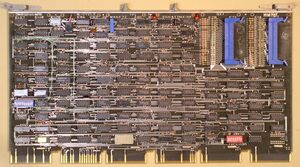
DR11-W Direct Memory Access Interface
The DR11-W Direct Memory Access Interface was a parallel interface for the UNIBUS, one which used DMA to transfer data to a user device. It was a single hex card (the M8716) replacement for the earlier multi-card DR11-B parallel interface. The DR11-W is somewhat program compatible with the DR11-B.
By appropriate manipulation of the control lines (below), the user device can do byte or word cycles on the bus, perform read-modify-write bus cycles, or do block 'burst' bus transfers. The DR11-W can also be operated by programmed I/O, potentially via interrupts.
Like the DR11-B, the interface between the DR11-W and the user device uses a number of unidirectional control lines (below), which control data transfer; and sets of three 'status' and 'control' lines, which appear in the Status and Command Register. Data going to the user device is buffered in a set of latches; data coming from the user device is also buffered, and is sampled and latched when i) the input buffer register (below) is read, or ii) either 'Cycle Request' input line is asserted.
The register addresses, interrupt vector, and other configuration (e.g. the polarity of the BUSY signal) are selected by setting DIP switches on the card.
Contents
Registers
| Register | Abbreviation | Address |
|---|---|---|
| Word Count Register | DRWC | 772410 |
| Bus Address Register | DRBA | 772412 |
| Control and Status Register | DRCSR | 772414 |
| Error and Information Register | DREIR | 772414 |
| Data Buffer Register | DRDB | 772416 |
Writes to the CSR/EIR address are always sent to the CSR. The result of a read depends on the setting of the Register Select bit, which is set by a write to the CSR.
The addresses shown are for the first DR11-W in a system; additional ones are normally set to be at 772430, 772450, 772470, etc.
In the register contents (below), bits which are read/write or unused are shown in normal font, those which are read-only are in italics, and write-only in bold.
772410: Word Count Register (DRWC)
| WC15 <---> WC00 | |||||||||||||||
| 15 | 14 | 13 | 12 | 11 | 10 | 09 | 08 | 07 | 06 | 05 | 04 | 03 | 02 | 01 | 00 |
Bit 0 is read-only, and is provided by the connected user device.
772412: Bus Address Register (DRBA)
| BA15 <---> BA00 | |||||||||||||||
| 15 | 14 | 13 | 12 | 11 | 10 | 09 | 08 | 07 | 06 | 05 | 04 | 03 | 02 | 01 | 00 |
Bit 0 is read-only, and is provided by the connected user device.
772414: Control and Status Register (DRCSR)
| ERROR/REGSEL | NXM | ATTN | MAINT | STAT A-C | CYCLE | READY | IE | XBA16-17 | FUNC1-3 | REGSEL/GO | |||||
| 15 | 14 | 13 | 12 | 11 | 10 | 09 | 08 | 07 | 06 | 05 | 04 | 03 | 02 | 01 | 00 |
772414: Error and Information Register (DREIR)
| ERROR | NXM | ATTN | MCR | ACLO | PAR | BRTE | NBS | Unused | REGSEL | ||||||
| 15 | 14 | 13 | 12 | 11 | 10 | 09 | 08 | 07 | 06 | 05 | 04 | 03 | 02 | 01 | 00 |
772416: Data Buffer Register (DRDB)
| Data15 <---> Data00 | |||||||||||||||
| 15 | 14 | 13 | 12 | 11 | 10 | 09 | 08 | 07 | 06 | 05 | 04 | 03 | 02 | 01 | 00 |
This is actually a pair of registers; a read-only input buffer register, and a write-only output buffer register.
Implementation
Connection to the user's device is via a pair of 40-pin Berg connector headers, into which flat cables (such as BC06R's) plug. For diagnostic purposes, a BC05L cable can be used to loop the device's input and output together.
Both receivers and drivers are single-ended, so for best results the DR11-W and the user's device should share a ground.
External links
- DR11-W Direct Memory Interface Module User's Guide (EK-DR11W-UG-001)
- DR11-W Direct Memory Access Interface Module User's Guide (EK-DR11W-UG-004)
- DR11-W Field Maintenance Print Set (MP00693)
