Difference between revisions of "PDP-11/05"
(→CPU board versions: Jumper locations) |
(Split out KD11-B) |
||
| Line 1: | Line 1: | ||
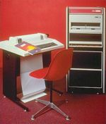
| − | [[Image:pdp11-05.jpg|150px| | + | [[Image:pdp11-05.jpg|150px|left|thumb|A PDP-11/05 from a sales brochure.]] |
{{Infobox Machine | {{Infobox Machine | ||
| Line 14: | Line 14: | ||
| caption = a PDP-11/05 from a sales brochure. --> | | caption = a PDP-11/05 from a sales brochure. --> | ||
| − | The '''PDP-11/05''' was the fourth | + | The '''PDP-11/05''' was the fourth model in the [[PDP-11]] series, following the [[PDP-11/20]], the [[PDP-11/45]] and the [[PDP-11/40]]; it used the [[KD11-B CPU]]. It was intended as a cost-reduced low-end machine to replace the PDP-11/20. Like all the other early PDP-11's, it was a [[UNIBUS]] machine. |
| − | The PDP-11/05 was identical to the [[PDP-11/10]]; the only difference between the /05 and the /10 was the number on the front panel. The /05 was aimed toward the [[OEM]] market, while the /10 was intended for end-users. General usage (following DEC's lead) is to refer to all these machines as '11/ | + | The PDP-11/05 was identical to the [[PDP-11/10]]; the only difference between the /05 and the /10 was the number on the front panel. The /05 was aimed toward the [[OEM]] market, while the /10 was intended for end-users. General usage (following DEC's lead) is to refer to all these machines as '11/05's. |
| − | |||
| − | |||
==Backplane versions== | ==Backplane versions== | ||
| − | The PDP-11/05 and /10 came in three versions, with different main | + | The PDP-11/05 and /10 came in three versions, with different main [[backplane]]s (the 9-slot unit holding the two [[Central Processing Unit|CPU]] cards). |
The original /05 and /10 came with backplanes wired to hold [[MM11-L]] 16 Kbyte core memory units. There were two different backplanes: one held two memory units, with one slot left for [[Small Peripheral Controller|SPC]] devices; the other held one memory unit, and provided four SPC slots. | The original /05 and /10 came with backplanes wired to hold [[MM11-L]] 16 Kbyte core memory units. There were two different backplanes: one held two memory units, with one slot left for [[Small Peripheral Controller|SPC]] devices; the other held one memory unit, and provided four SPC slots. | ||
| Line 29: | Line 27: | ||
The later /05S and /10S came with a backplane wired to hold an [[MM11-U]] 32 Kbyte core memory, and which provided three SPC slots. | The later /05S and /10S came with a backplane wired to hold an [[MM11-U]] 32 Kbyte core memory, and which provided three SPC slots. | ||
| − | |||
| − | |||
| − | |||
| − | |||
| − | |||
| − | |||
| − | |||
| − | |||
| − | |||
| − | |||
| − | |||
| − | |||
| − | |||
| − | |||
| − | |||
| − | |||
| − | |||
| − | |||
| − | |||
| − | |||
| − | |||
| − | |||
| − | |||
| − | |||
| − | |||
| − | |||
| − | |||
| − | |||
| − | |||
| − | |||
| − | |||
| − | |||
| − | |||
| − | |||
| − | |||
| − | |||
| − | |||
| − | |||
| − | |||
| − | |||
| − | |||
| − | |||
| − | |||
| − | |||
| − | |||
| − | |||
| − | |||
| − | |||
| − | |||
| − | |||
| − | |||
| − | |||
| − | |||
| − | |||
| − | |||
| − | |||
| − | |||
| − | |||
| − | |||
| − | |||
| − | |||
| − | |||
| − | |||
| − | |||
| − | |||
| − | |||
| − | |||
| − | |||
| − | |||
| − | |||
| − | |||
| − | |||
| − | |||
| − | |||
| − | |||
| − | |||
| − | |||
| − | |||
| − | |||
| − | |||
| − | |||
| − | |||
| − | |||
| − | |||
| − | |||
| − | |||
| − | |||
| − | |||
| − | |||
| − | |||
| − | |||
| − | |||
| − | |||
| − | |||
| − | |||
| − | |||
| − | |||
| − | |||
| − | |||
| − | |||
| − | |||
| − | |||
| − | |||
| − | |||
| − | |||
| − | |||
| − | |||
| − | |||
| − | |||
| − | |||
| − | |||
| − | |||
| − | |||
| − | |||
| − | |||
| − | |||
| − | |||
| − | |||
| − | |||
| − | |||
| − | |||
| − | |||
| − | |||
| − | |||
| − | |||
| − | |||
| − | |||
| − | |||
| − | |||
| − | |||
| − | |||
| − | |||
| − | |||
| − | |||
| − | |||
| − | |||
| − | |||
| − | |||
| − | |||
==Keys== | ==Keys== | ||
| Line 179: | Line 38: | ||
{{PDP-11}} | {{PDP-11}} | ||
| − | |||
| − | |||
| − | |||
Revision as of 15:41, 12 February 2018
| PDP-11/05 | |
| Manufacturer: | Digital Equipment Corporation |
|---|---|
| Architecture: | PDP-11 |
| Year Introduced: | June 1972 |
| Word Size: | 16 bit |
| Physical Address Size: | 18 bit (only 16 bits usable) |
| Bus Architecture: | UNIBUS |
The PDP-11/05 was the fourth model in the PDP-11 series, following the PDP-11/20, the PDP-11/45 and the PDP-11/40; it used the KD11-B CPU. It was intended as a cost-reduced low-end machine to replace the PDP-11/20. Like all the other early PDP-11's, it was a UNIBUS machine.
The PDP-11/05 was identical to the PDP-11/10; the only difference between the /05 and the /10 was the number on the front panel. The /05 was aimed toward the OEM market, while the /10 was intended for end-users. General usage (following DEC's lead) is to refer to all these machines as '11/05's.
Backplane versions
The PDP-11/05 and /10 came in three versions, with different main backplanes (the 9-slot unit holding the two CPU cards).
The original /05 and /10 came with backplanes wired to hold MM11-L 16 Kbyte core memory units. There were two different backplanes: one held two memory units, with one slot left for SPC devices; the other held one memory unit, and provided four SPC slots.
A second version, the /05N and /10N, came in a 10-1/2 inch box and had a slightly different backplane, which had space for two MM11-L memory units, but deleted the SPC slot of the previous double MM11-L backplane, and replaced it with a slot to hold the dual-height M9970 console terminal cable board.
The later /05S and /10S came with a backplane wired to hold an MM11-U 32 Kbyte core memory, and which provided three SPC slots.
Keys
Unlike all the other keyed PDP-11s, which use a circular Ace key, the /05's (and /10s) use a normal flat Yale-type key. The original key is a Chicago Lock Company key, code "GRB 2"; this is cut 215, on a Chicago K5K or Ilco S1041T blank. If simply duplicating an existing key, Hillman Y11 and FR4 blanks may be used (both work, but one has to be trimmed a bit, length-wise).
Gallery
| v • d • e PDP-11 Computers and Peripherals |
|---|
| UNIBUS PDP-11s - PDP-11/20 • PDP-11/15 • PDP-11/35 • PDP-11/40 • PDP-11/45 • PDP-11/50 • PDP-11/55 • PDP-11/70 PDP-11/05 • PDP-11/10 • PDP-11/04 • PDP-11/34 • PDP-11/60 • PDP-11/44 • PDP-11/24 • PDP-11/84 • PDP-11/94 QBUS PDP-11s - PDP-11/03 • PDP-11/23 • PDP-11/23+ • MicroPDP-11/73 • MicroPDP-11/53 • MicroPDP-11/83 • MicroPDP-11/93 QBUS CPUs: LSI-11 • LSI-11/2 • KDF11-A • KDF11-B • KDJ11-A • KDJ11-B • KDJ11-D • KDJ11-E Buses: UNIBUS • UNIBUS map • SPC • MUD • EUB • QBUS • CD interconnect • PMI Also: PDP-11 architecture • PDP-11 Extended Instruction Set • FP11 floating point • PDP-11 Memory Management |
| UNIBUS CPUs: KA11 • KC11 • KB11-A • KB11-B • KB11-C • KB11-D • KD11-A • KD11-B • KD11-D • KD11-E • KD11-EA • KD11-K • KD11-Z • KDF11-U
Co-processors: FP11-A • FP11-B • FP11-C • FP11-E • FP11-F • KE44-A • FPF11 Chips: LSI-11 • KEV11-A • KEV11-B • KEV11-C • F-11 • KEF11-A • KTF11-A • T-11 • J-11 • FPJ11 CPU options: KE11-E • KE11-F • KJ11-A • KT11-C • KT11-D • KK11-A • KK11-B • KT24 • KTJ11-B Rare CPU options: KS11 Memory Protection and Relocation option • KT11-B Paging Option • KUV11 Writeable Control Store Front panels: KY11-A • KY11-D • KY11-J • KY11-LA • KY11-LB • KY11-P More on buses: UNIBUS and QBUS termination • Bus Arbitration on the Unibus and QBUS • CTI BUS PDT-11s - PDT-11/110 • PDT-11/130 • PDT-11/150 CTI PDP-11s - PRO-325 • PRO-350 • PRO-380 Other: FIS floating point • PDP-11 Commercial Instruction Set • PDP-11 stacks • PDP-11 family differences |


