Difference between revisions of "KT11-B Technical Manual"
(→Drawing Conventions: add latching mux) |
m (→States: clarify) |
||
| Line 61: | Line 61: | ||
==States== | ==States== | ||
| − | The KT11-B has a state composed of two parts, the 'X' or major part, and the 'Y' or minor part. | + | The KT11-B has a state composed of two parts, the 'X' or major part, and the 'Y' or minor part; the progression of this through the various states is the major control mechanism in the KT11-B. |
The X state counter is on print 12; it is composed of a 2-bit counter composed of a pair of D flops, with 4 AND gates with inverting inputs to create individual major state outputs, signals 'XSRx' (x = 0-3). | The X state counter is on print 12; it is composed of a 2-bit counter composed of a pair of D flops, with 4 AND gates with inverting inputs to create individual major state outputs, signals 'XSRx' (x = 0-3). | ||
| − | The Y state counter is an M826 Flip Chip, showm on print 8; its outputs are signals 'YSRx' (x = 0,1,3,7,15,14,12,8). | + | The Y state counter is an M826 Flip Chip, showm on print 8; its outputs are signals 'YSRx' (x = 0, 1 ,3, 7, 15, 14, 12, 8). (The odd sequence of minor state numbers, and the fact that they are not in numerical order, ''is'' confusing, but since that's what's on the prints, that nomenclature has to be used.) |
| − | The two groups of signals are combined into signals for each individual major/minor state by NAND gates shown on drawing 12; inverters provide non-inverted forms. | + | The two groups of signals are combined into signals which indicate that the KT11-B is in that state, for each individual major/minor state, by NAND gates shown on drawing 12; inverters then provide non-inverted forms of each. |
Revision as of 17:03, 9 September 2016
As a Special Systems Option, the KT11-B does not have the usual DEC Technical Manual. This page attempts to provide at least the high-level portions of such a manual.
Prints
The Engineering Drawings for the KT11-B (7605071) include the following logic prints:
| Number | Page Count | Content |
|---|---|---|
| 2 | 2 | Address Bus and Control Logic |
| 3 | 1 | State Control Logic |
| 4 | 1 | SP Input Mux |
| 5 | 2 | Associative Memory Control |
| 6 | 1 | Scratch Pad and State Control Logic |
| 7 | 3 | Data Bus and Control Logic |
| 8 | 1 | Keys and Associative Memory |
| 9 | 1 | XP Option for KT11 Associative Memory Control |
| 10 | 1 | PGM Register |
| 11 | 1 | PGC Register |
| 12 | 1 | Timing Logic |
| 13 | 1 | Buffered Signals and Main Logic |
| 14 | 1 | Extended Associative Memory |
| 15 | 1 | KA11 to KT11 Interface |
| 17 | 1 | KT11-B Bus Connectors |
Drawing Conventions
The drawings are somewhat easier to understand if the conventions used in the drawings are understood. Although no document lists them, they can be ascertained by study of the drawings.
Signal Names
Signal names in this drawing set usually start with 'Dxx', where 'xx' is the drawing number (given in the table above). Inverted (asserted low) signals are shown as '-XXX'. In signal names of the form 'XXX (yy)', 'yy' is a bit number (in standard PDP-11 order) in a register or bus.
The following specific signal names have the meaning given:
- Signals of the form 'x.y' are states, with 'x' being the major state, and 'y' being the minor state.
Common Circuits
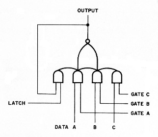
This circuit (first used in the KA11) is seen in several places in the KT11-B. It is almost always seen as an array of identical circuits, since it provides a 3-input multiplexor with latching capability, and it is used on data paths (usually 16 bits wide).
The latch is cleared by de-asserting the 'Latch' input; data from any of the three inputs (A, B, C) may then be selected for output, and potentially storage, by asserting the matching 'Gate' input. Asserting 'Latch' then stores the current output of the mux.
States
The KT11-B has a state composed of two parts, the 'X' or major part, and the 'Y' or minor part; the progression of this through the various states is the major control mechanism in the KT11-B.
The X state counter is on print 12; it is composed of a 2-bit counter composed of a pair of D flops, with 4 AND gates with inverting inputs to create individual major state outputs, signals 'XSRx' (x = 0-3).
The Y state counter is an M826 Flip Chip, showm on print 8; its outputs are signals 'YSRx' (x = 0, 1 ,3, 7, 15, 14, 12, 8). (The odd sequence of minor state numbers, and the fact that they are not in numerical order, is confusing, but since that's what's on the prints, that nomenclature has to be used.)
The two groups of signals are combined into signals which indicate that the KT11-B is in that state, for each individual major/minor state, by NAND gates shown on drawing 12; inverters then provide non-inverted forms of each.
