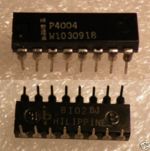
Intel 4004
The Intel 4004 microprocessor was the first commercially available microprocessor (although not Intel's first microprocessor design; work had started on what became the Intel 8008 first). It was designed by Federico Faggin, who in 1974 left Intel and started Zilog. (Interestingly, Fagin 'signed' his work; the chip contains an "F.F." in one corner.)
Contents
Details
The 4004 came in a 16-pin DIP[1] chip, and had limitations when compared to later microprocessors. It could only execute code out of ROM, RAM was only used for storing data, and this complicated the life of the programmer somewhat.
It seems to have limited support for off-chip RAM. The 16 4-bit-wide internal registers seem to be the primary locations for writing data; there is no 'store' instruction. But the SRC instruction seems to send an address out, for later used by the Wxx instructions. (Also, the CM-RAM[0123] lines from the processor chip are used to control "4002 RAM chips".)
Data and address information were multiplexed on a 4-bit bus. The need to multiplex the bus was part of the constraints caused by using a 16-pin DIP (40-pin DIPs were already in use by competitors at the time), enforced by Intel's management. Multiplexing reduced the instruction execution speed that could have been achieved, for example. The chip also needed a lot of support logic.
The 4004 was only the processor part of the chip set produced for the original client (Busicom; below). The original setup was known as 'The 4000 Family', AKA the 'Busicom Chip Set', AKA the 'MCS-4 Chip Set' and consisted of:
- The processor (the 4004)
- 2048-bit ROM, with a 4-bit programmable I/O port (the 4001)
- 320-bit RAM arranged in 4 'registers' containing 20 locations of 4-bit 'characters'; also a 4-bit output port (the 4002)
- A shift register type memory with serial input and parallel output (the 4003)
[1] Note: The BYTE article incorrectly stated that the chip came in an 18-pin DIP.
Width
The 4004 is often considered a '4-bit' chip, but the discussion is complicated; made even more confusing because there is no universally accepted standard for what sets a machine's 'width'. Indeed, for most suggested benchmarks, one can find a machine which violates it:
- address space (KA10; 18 bits - 36 bit machine)
- instruction size (Motorola M68000 family; 16 bits - 32 bit machine)
- bus width (Motorola MC68000; 16 bits - 32 bit machine)
- ALU width (LSI-11; 8 bits - 16 bit machine)
On a number of these metrics, the 4004 is actually sort of an 8-bit machine:
- Instructions are all multiples of 8 bits long
- Instruction addresses (in some jumps, etc) are 8 bits long (although there is one in which they are 12 bits)
- Immediate data is sometimes 8 bits wide
- Register pairs, the target of 'load immediate' instructions, are 8 bits wide
- Some data is 8 bits wide (in the FIN instruction, the data goes to a register pair, so 8 bits wide)
On the other hand:
- The accumulator is only 4 bits wide
- The ALU (and thus all data handling in arithmetic instructions) is only 4 bits wide
- Some data is 4 bits wide (it's not clear if in the LDM instruction, the 'DDDD' bits are immediate data, or the address of the data [probably immediate]; either way, it goes to the accumulator, so only 4 bits wide)
So, it's truly a mix.
History
The 4004 resulted when the Japanese company Busicom contracted Intel in 1969 to create a chip set for a printer-calculator.
Busicom eventually permitted Intel to use the chipset design for non-calculator applications (the year this happened was 1971, according to sources). The processor chip was eventually called the 4004 and sold for $200.
External links
- MCS4 - documentation at Bitsavers
- MCS-4 Micro Computer Set Users Manual - all the chips in the set (4001 ROM; 4002 RAM; etc)
- 4004 Single Chip 4-Bit P-Channel Microprocessor - data sheet with detailed specifications
- Oral History Panel on the Development and Promotion of the Intel 4004 Microprocessor
- The Intel 4004 Microprocessor and the Silicon Gate Technology
- Intel 4004 — 50th Anniversary Project
- The Texas Instruments TMX 1795: the (almost) first, forgotten microprocessor - Ken Shirriff's article about the first microprocessors, covers the 4004 also
- Volume 3, number 7, July 1978, "The First Ten Years of Amateur Computing"
