Difference between revisions of "MM11-L core memory"
(+images) |
m (→External links: +ME11/MF11 prints) |
||
| (5 intermediate revisions by the same user not shown) | |||
| Line 1: | Line 1: | ||
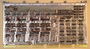
| + | [[Image:MM11-L_G110.jpg|thumb|300px|right|G110 control logic board; the blank area in the center right holds the extra components for the parity bits in the G109 variant]] | ||
| + | |||
The '''MM11-L core memory''' was a popular, and common, 16 Kbyte [[core memory|core]] [[main memory]] unit for the early [[PDP-11]] [[UNIBUS]] machines. An MM11-L was composed of a three board set: | The '''MM11-L core memory''' was a popular, and common, 16 Kbyte [[core memory|core]] [[main memory]] unit for the early [[PDP-11]] [[UNIBUS]] machines. An MM11-L was composed of a three board set: | ||
| − | |||
| − | |||
* G110 - [[DEC card form factor|hex-width]] memory control logic and data channels | * G110 - [[DEC card form factor|hex-width]] memory control logic and data channels | ||
| Line 7: | Line 7: | ||
* H214 - quad-width core stack | * H214 - quad-width core stack | ||
| − | The MM11-L required a custom [[backplane]], although some [[Central Processing Unit|CPU]]'s (e.g. the [[PDP-11/05]]) had processor backplanes wired to hold one or more MM11-L sets, in addition to the CPU. | + | The MM11-L required a custom [[backplane]], although some [[Central Processing Unit|CPU]]'s (e.g. the [[PDP-11/05]]) had processor backplanes wired to hold one or more MM11-L sets, in addition to the [[Central Processing Unit|CPU]]. |
The '''MM11-S''' was a four-slot backplane plus a single MM11-L board set. The '''MF11-L''' was a nine-slot backplane plus a single MM11-L board set; the backplane has room for two more MM11-L board sets. The '''ME11-L''' was an MF11-L in a 5-1/4" rack-mount box, with [[power supply]] (the -LA was wired for 115V supply, the -LB for 230V). | The '''MM11-S''' was a four-slot backplane plus a single MM11-L board set. The '''MF11-L''' was a nine-slot backplane plus a single MM11-L board set; the backplane has room for two more MM11-L board sets. The '''ME11-L''' was an MF11-L in a 5-1/4" rack-mount box, with [[power supply]] (the -LA was wired for 115V supply, the -LB for 230V). | ||
| + | |||
| + | The G231 board of the MM11-L is also used, with the 19-bit wide H216 variant of the core stack, in the [[MF10 core memory]]. | ||
==Parity== | ==Parity== | ||
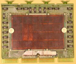
| − | [[Image: | + | [[Image:H215-core-memory-board.jpg|thumb|250px|right|H215 parity core memory board]] |
| − | There was also a [[parity]] variant, the '''MM11-LP'''; parity versions (denoted by a 'P' suffix) were available for all of the above. The MM11-LP added a dual-width [[M7259 Parity Control Module]], and substituted an H215 (with two more bits per word) for the H214, and a G109 for the G110. (The G109 and G110 use the same [[ | + | There was also a [[parity]] variant of the MM11-L, the '''MM11-LP'''; parity versions (denoted by a 'P' suffix) were available for all of the above. The MM11-LP added a dual-width [[M7259 Parity Control Module]], and substituted an H215 (with two more bits per word - for byte parity) for the H214, and a G109 for the G110. (The G109 and G110 use the same [[etch]]; the G110 omits the components for the two parity bits.) Enabling parity increased the [[access time]] from 400 nsec to 525 nsec. |
| − | The manual indicates that an 'MF11-LP backplane' was required, but it is not stated if this version had a different [[printed circuit board|PCB]], or if the non-parity version simply had a [[jumper]], like the [[MM11-U core memory]]. After some investigation, apparently there were two versions of the backplane, the early one (part | + | The manual indicates that an 'MF11-LP backplane' was required, but it is not stated if this version had a different [[printed circuit board|PCB]], or if the non-parity version simply had a [[jumper]], like the [[MM11-U core memory]]. After some investigation, apparently there were two versions of the backplane, the early one ([[DEC part number]] 54-09959) which cannot run parity, and a later one (part number 54-10331) which can. An example of the later backplane had the same jumper as that called for for the MM11-U, from pin 1BU1 to 2BU1; this jumper should not be present for parity memory. |
The parity controller, if present, can only be placed in slot 6. The backplane connects together all the BU1 SSYN pins on the interior slots (2-8), effectively an 'internal' SSYN; the jumper connects together that line, and the main UNIBUS SSYN. The G109/G110 modules drive that 'internal' SSYN; hence the need to install the jumper for non-parity memory. When parity is enabled, the parity controller drives the bus SSYN via pin BV2 in its slot, which is directly connected to bus SSYN via a [[trace]]; the controller uses the 'internal' SSYN as input. | The parity controller, if present, can only be placed in slot 6. The backplane connects together all the BU1 SSYN pins on the interior slots (2-8), effectively an 'internal' SSYN; the jumper connects together that line, and the main UNIBUS SSYN. The G109/G110 modules drive that 'internal' SSYN; hence the need to install the jumper for non-parity memory. When parity is enabled, the parity controller drives the bus SSYN via pin BV2 in its slot, which is directly connected to bus SSYN via a [[trace]]; the controller uses the 'internal' SSYN as input. | ||
| Line 54: | Line 56: | ||
The first MM11-L set goes in slots 1/2/3; as MM11-L sets were added, they were installed in slot numerical order. (The location of the parity controller is the only un-used dual slot in a full MF11-L.) | The first MM11-L set goes in slots 1/2/3; as MM11-L sets were added, they were installed in slot numerical order. (The location of the parity controller is the only un-used dual slot in a full MF11-L.) | ||
| + | |||
| + | ==See also== | ||
| + | |||
| + | * [[MM11-K core memory]] | ||
| + | |||
| + | ==External links== | ||
| + | |||
| + | * [http://shop-pdp.net/~stuff/PDFs/DEC/DEC-11-HMELA-B-D_ME11-L_Core_Memory_System_Manual.pdf ME11-L core memory system manual] (DEC-11-HMELA-B-D) | ||
| + | * [http://www.bitsavers.org/www.computer.museum.uq.edu.au/pdf/DEC-11-HMFLA-C-D%20MM11-S,%20MF11-L,%20and%20MF11-LP%20core%20memory%20systems.pdf MM11-S, MF11-L, and MF11-LP core memory systems] (DEC-11-HMFLA-C-D) | ||
| + | * [http://bitsavers.org/pdf/dec/pdp11/1105/1105_RevAH_Engineering_Drawings_Jul76.pdf PDP-11/05 Engineering Drawings] - contains complete engineering drawings for the MM11-L board set on pp. 115-137 | ||
| + | * [https://archive.org/details/dec-me-11-l-core-memory-system-engineering-drawings/ ME11-L core memory system engineering drawings] | ||
[[Category: UNIBUS Memories]] | [[Category: UNIBUS Memories]] | ||
Latest revision as of 05:14, 25 March 2022
The MM11-L core memory was a popular, and common, 16 Kbyte core main memory unit for the early PDP-11 UNIBUS machines. An MM11-L was composed of a three board set:
- G110 - hex-width memory control logic and data channels
- G231 - hex-width memory driver logic
- H214 - quad-width core stack
The MM11-L required a custom backplane, although some CPU's (e.g. the PDP-11/05) had processor backplanes wired to hold one or more MM11-L sets, in addition to the CPU.
The MM11-S was a four-slot backplane plus a single MM11-L board set. The MF11-L was a nine-slot backplane plus a single MM11-L board set; the backplane has room for two more MM11-L board sets. The ME11-L was an MF11-L in a 5-1/4" rack-mount box, with power supply (the -LA was wired for 115V supply, the -LB for 230V).
The G231 board of the MM11-L is also used, with the 19-bit wide H216 variant of the core stack, in the MF10 core memory.
Contents
Parity
There was also a parity variant of the MM11-L, the MM11-LP; parity versions (denoted by a 'P' suffix) were available for all of the above. The MM11-LP added a dual-width M7259 Parity Control Module, and substituted an H215 (with two more bits per word - for byte parity) for the H214, and a G109 for the G110. (The G109 and G110 use the same etch; the G110 omits the components for the two parity bits.) Enabling parity increased the access time from 400 nsec to 525 nsec.
The manual indicates that an 'MF11-LP backplane' was required, but it is not stated if this version had a different PCB, or if the non-parity version simply had a jumper, like the MM11-U core memory. After some investigation, apparently there were two versions of the backplane, the early one (DEC part number 54-09959) which cannot run parity, and a later one (part number 54-10331) which can. An example of the later backplane had the same jumper as that called for for the MM11-U, from pin 1BU1 to 2BU1; this jumper should not be present for parity memory.
The parity controller, if present, can only be placed in slot 6. The backplane connects together all the BU1 SSYN pins on the interior slots (2-8), effectively an 'internal' SSYN; the jumper connects together that line, and the main UNIBUS SSYN. The G109/G110 modules drive that 'internal' SSYN; hence the need to install the jumper for non-parity memory. When parity is enabled, the parity controller drives the bus SSYN via pin BV2 in its slot, which is directly connected to bus SSYN via a trace; the controller uses the 'internal' SSYN as input.
Note that therefore parity and non-parity memory cannot be mixed on the same backplane. There is also no provision for use of the M7259 parity controller in the PDP-11/05 backplanes which support the MM11-L.
(One could probably easily ECO the earlier version backplane to support parity, since the SSYN trace is accessible: cut the trace at 1BU1 and 9BU1, and add the needed wire-wrap lines.)
Module chart
The board organization in the MM11-L backplanes is not given in the manual; that for the MF11-L is:
| Connector | ||||||
|---|---|---|---|---|---|---|
| Slot | A | B | C | D | E | F |
| 1 | UNIBUS In | H213/H214 Core stack | ||||
| 2 | G231 Memory Driver | |||||
| 3 | G110 Memory Control | |||||
| 4 | G231 Memory Driver | |||||
| 5 | G110 Memory Control | |||||
| 6 | M7259 Parity Controller | H213/H214 Core stack | ||||
| 7 | G231 Memory Driver | |||||
| 8 | G110 Memory Control | |||||
| 9 | UNIBUS Out | H213/H214 Core stack | ||||
The first MM11-L set goes in slots 1/2/3; as MM11-L sets were added, they were installed in slot numerical order. (The location of the parity controller is the only un-used dual slot in a full MF11-L.)
See also
External links
- ME11-L core memory system manual (DEC-11-HMELA-B-D)
- MM11-S, MF11-L, and MF11-LP core memory systems (DEC-11-HMFLA-C-D)
- PDP-11/05 Engineering Drawings - contains complete engineering drawings for the MM11-L board set on pp. 115-137
- ME11-L core memory system engineering drawings

