Difference between revisions of "KD11-B CPU"
(Split out from -11/05 page) |
m (rm bloat) |
||
| (6 intermediate revisions by the same user not shown) | |||
| Line 1: | Line 1: | ||
| − | The '''KD11-B''' [[PDP-11]] [[Central Processing Unit|CPU]] for the [[PDP-11/05]] and [[PDP-11/10]] was a two-board [[ | + | The '''KD11-B''' [[PDP-11]] [[Central Processing Unit|CPU]] for the [[PDP-11/05]] and [[PDP-11/10]] was a two-board [[microcode|micro-programmed]] processor contained on two [[DEC card form factor|hex]] cards. The basic micro-code was 40 bits wide, including 8 bits of 'next micro-[[instruction]] [[address]]', 4 bits of '[[jump|branch]] micro-test', and 5 bits of '[[arithmetic logic unit|ALU]] control'. |
Like other early, low-cost PDP-11s, it did not support either hardware [[floating point]], or [[PDP-11 Extended Instruction Set|EIS]]. It did include an [[asynchronous serial line]] console port, but only [[20mA current loop serial line interface|20mA physical layer]]. | Like other early, low-cost PDP-11s, it did not support either hardware [[floating point]], or [[PDP-11 Extended Instruction Set|EIS]]. It did include an [[asynchronous serial line]] console port, but only [[20mA current loop serial line interface|20mA physical layer]]. | ||
==CPU board versions== | ==CPU board versions== | ||
| + | |||
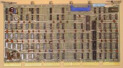
| + | [[Image:KD11-B M7260C.jpg|250px|right|thumb|A KD11-B M7260 Data Paths card, etch revision C]] | ||
The two boards in the KD11-B (the M7260 Data Paths module, and the M7261 Control Logic module) both come in two markedly-different versions, but unlike later practise (as in, e.g. the [[PDP-11/34]]), the two versions are not given different M-numbers, or clearly marked with a revision (i.e. 'M7260' and 'M7260-YA') on the handles. | The two boards in the KD11-B (the M7260 Data Paths module, and the M7261 Control Logic module) both come in two markedly-different versions, but unlike later practise (as in, e.g. the [[PDP-11/34]]), the two versions are not given different M-numbers, or clearly marked with a revision (i.e. 'M7260' and 'M7260-YA') on the handles. | ||
| − | One easy way to visually distinguish the early M7260 from later ones is that the later ones contain a circular selector switch in the upper left corner to select the baud rate of the built-in serial line; also, the position of the large [[UART]] chip has a different location (from down near the contact fingers, to up near the handles) and orientation ( | + | ''Supplement 2: Description of data paths module M7260 revision M'' to the ''PDP-11/05, 11/10 computer manual'' (below) says that "All revisions of the M7260 module are functionally interchangeable"; ''Supplement 3: Description of control logic and microprogram module M7261 revision R'' makes a similar statement about the M7261. Whether this means that a unit composed of an early M7260 and a late M7261 will operate properly has not been confirmed by actual experimentation, but that is the likely import of this statement (and not merely that they operate in a similar way); similarly, for a late M7260 and an early M7261. |
| + | |||
| + | One easy way to visually distinguish the early M7260 from later ones is that the later ones (image at right) contain a circular selector switch in the upper left corner to select the baud rate of the built-in serial line; also, the position of the large [[UART]] chip has a different location (from down near the contact fingers, to up near the handles) and orientation (parallel to the board's long axis, in the earlier revision). | ||
| + | |||
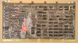
| + | For the M7261, the early version of the board (image below) has a large blank area, containing only traces, in the left middle area of the board. The early version also has the traces laid out by hand; the later is automagically routed. | ||
| + | |||
| + | [[Image:KD11-B M7261E.jpg|250px|left|thumb|A KD11-B M7261 Control Logic card, etch revision E]] | ||
The early revision of the M7260 is the 'B' revision; the later is the 'C' revision (the latter is marked as such, on the back side of the board- "M7260C"). For the M7261, two early revisions are the 'C' and 'E' revisions (the latter also similarly marked - "M7261E"); the later is the 'F' (also marked). | The early revision of the M7260 is the 'B' revision; the later is the 'C' revision (the latter is marked as such, on the back side of the board- "M7260C"). For the M7261, two early revisions are the 'C' and 'E' revisions (the latter also similarly marked - "M7261E"); the later is the 'F' (also marked). | ||
| Line 14: | Line 22: | ||
===Jumpers=== | ===Jumpers=== | ||
| + | |||
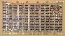
| + | [[Image:KD11-B M7261F.jpg|250px|right|thumb|A KD11-B M7261 Control Logic card, etch revision F]] | ||
The later revision of the M7261 contains two jumpers which are not present on the earlier revision. | The later revision of the M7261 contains two jumpers which are not present on the earlier revision. | ||
| Line 142: | Line 152: | ||
|} | |} | ||
| − | + | ==External links== | |
| + | |||
| + | * [http://www.bitsavers.org/pdf/dec/pdp11/1105/EK-KD11B-MM-001_Jan75.pdf KD11-B processor maintenance manual] (EK-KD11B-MM-001) | ||
| + | * [http://bitsavers.org/pdf/dec/pdp11/1105/DEC-11-H05AA-A-D_1105um.pdf PDP-11/05 computer manual] (DEC-11-H05AA-A-D) - covers the KD11-B in ''Part II: KD11-B Processor'' (pp. 70-193 of the PDF) | ||
| + | * [http://www.bitsavers.org/www.computer.museum.uq.edu.au/pdf/DEC-11-H05AA-B-D%20PDP-11-05,%2011-10%20Computer%20Manual.pdf PDP-11/05, 11/10 computer manual] (DEC-11-H05AA-B-D) - covers the details of the differences between the two generations of CPU cards in ''Supplement 2: Description of data paths module M7260 revision M'' and ''Supplement 3: Description of control logic and microprogram module M7261 revision R'' (pp. 373-392 of the PDF) | ||
| + | * [http://www.bitsavers.org/pdf/dec/pdp11/1105/1105_RevAH_Engineering_Drawings_Jul76.pdf 16 bit computer (PDP 1105) engineering drawings, Revision AH] (covers the KD11-B on pp. 21-113 of the PDF) | ||
| + | * [http://www.bitsavers.org/pdf/dec/pdp11/1105/1105S_Schem.pdf PDP-11/05-S, 11/10-S systems engineering drawings, Revision D] (covers the KD11-B on pp. 11-103 of the PDF) | ||
| − | [[Category:PDP-11 | + | [[Category: PDP-11 UNIBUS Processors]] |
| − | |||
Latest revision as of 19:07, 2 July 2023
The KD11-B PDP-11 CPU for the PDP-11/05 and PDP-11/10 was a two-board micro-programmed processor contained on two hex cards. The basic micro-code was 40 bits wide, including 8 bits of 'next micro-instruction address', 4 bits of 'branch micro-test', and 5 bits of 'ALU control'.
Like other early, low-cost PDP-11s, it did not support either hardware floating point, or EIS. It did include an asynchronous serial line console port, but only 20mA physical layer.
CPU board versions
The two boards in the KD11-B (the M7260 Data Paths module, and the M7261 Control Logic module) both come in two markedly-different versions, but unlike later practise (as in, e.g. the PDP-11/34), the two versions are not given different M-numbers, or clearly marked with a revision (i.e. 'M7260' and 'M7260-YA') on the handles.
Supplement 2: Description of data paths module M7260 revision M to the PDP-11/05, 11/10 computer manual (below) says that "All revisions of the M7260 module are functionally interchangeable"; Supplement 3: Description of control logic and microprogram module M7261 revision R makes a similar statement about the M7261. Whether this means that a unit composed of an early M7260 and a late M7261 will operate properly has not been confirmed by actual experimentation, but that is the likely import of this statement (and not merely that they operate in a similar way); similarly, for a late M7260 and an early M7261.
One easy way to visually distinguish the early M7260 from later ones is that the later ones (image at right) contain a circular selector switch in the upper left corner to select the baud rate of the built-in serial line; also, the position of the large UART chip has a different location (from down near the contact fingers, to up near the handles) and orientation (parallel to the board's long axis, in the earlier revision).
For the M7261, the early version of the board (image below) has a large blank area, containing only traces, in the left middle area of the board. The early version also has the traces laid out by hand; the later is automagically routed.
The early revision of the M7260 is the 'B' revision; the later is the 'C' revision (the latter is marked as such, on the back side of the board- "M7260C"). For the M7261, two early revisions are the 'C' and 'E' revisions (the latter also similarly marked - "M7261E"); the later is the 'F' (also marked).
The early version of the M7260 only supports 110 baud operation; the latter has a circular selector switch which allows operation at a range of speeds from 110 baud up to 2400 baud; however, it is necessary to tweak a trim pot to change from the 110/220/440/880/1760 speed set to the 150/300/600/1200/2400 set.
Jumpers
The later revision of the M7261 contains two jumpers which are not present on the earlier revision.
One (W1), when installed, disables the built-in serial line (which is 20mA, and limited to 2400 baud), allowing use of a more capable serial interface as the system console. The other (W2), when installed, disables the CPU from acting as a bus arbitrator, so that the machine can be a 'slave' processor, on a UNIBUS controlled by another CPU.
They are not labeled, which makes them impossible to find without external information. With the board component face up, and the contact fingers at the bottom, W1 is immediately to the right of E69, and W2 is immediately to the right of E73.
Control PROMs
The KD11-B makes extensive use of PROMs in place of random logic for control purposes; both boards contain a large number of PROMs, in 32x8 and 256x4 formats.
The two types used on the M7260 are Intersil IM5600 32x8 PROM (IM5600C or equivalent; DEC also used MMI 6630C's, and Signetics N8223B's); and the 74187 256x4 PROM (DEC also used Intersil IM5603C's, and MMI 6108's and 4107's).
On the M7261, the IM5600 was used (DEC also used Signetics N82S23N's and N8223B's, and MMI 6330-1's), along with the Intersil IM5603 256x4 PROM (DEC also used Signetics 82S26N's [possibly a mis-print on the chip] and 82S126N's, MMI 6300-1's, 6300D's, 6111's and 6116's, and National DM74S387N's).
For the M7260 Data Paths board, the following table provides information on the PROMs on the early version (etch revision B) and late version (etch revision C). On the later version, the parts are all the same parts as the previous revision, but the chip numbering system for the board has been completely revised.
| Part # | Type | Rev. B | Rev. C |
|---|---|---|---|
| A01A1 | 32x8 | E25 | E44 |
| A02A1 | 32x8 | E53 | |
| A03A1 | 32x8 | E61 | E54 |
| A03A2 | 256x4 | E59 | E72 |
| A04A1 | 32x8 | E64 | E65 |
| A05A1 | 32x8 | E66 | E59 |
| A06A1 | 32x8 | E68 | E66 |
| A08A1 | 32x8 | E69 | E78 |
| A10A1 | 32x8 | E71 | E77 |
| A11A1 | 32x8 | E74 | E83 |
| A12A1 | 32x8 | E82 | E69 |
For the M7261 Control Logic and Microprogram board, the following table provides information on the PROMs on the early version (etch revisions C and E) and late version (etch revision F). On the later version, the parts are mostly the same parts as the previous revision, but the chip numbering system for the board has been completely revised.
| Function | Type | Part # | Rev. C | Rev. E | Rev. F |
|---|---|---|---|---|---|
| Bus Request -> Grant processing | 256x4 | A01A2 | E12 | E24 | |
| Internal address decode (first stage) | 256x4 | A02A2 | E30 | E53 | |
| Microprogram - Next instruction (high bits) | 256x4 | A04A2 | E92 | E102 | |
| Microprogram - Processor Status Word control | 256x4 | A05A2 | E93 | E104 | |
| Internal address decode (second stage) | 32x8 | A07A1 | E68 | E71 | |
| Microprogram - Bus control | 256x4 | A07A2 | E95 | ||
| A17A2 | E95 | E106 | |||
| Internal address decode (second stage) | 32x8 | A09A1 | E69 | E72 | |
| Branch utest service | 256x4 | A09A2 | E101 | E107 | |
| Microprogram - Next instruction (low bits) | 256x4 | A10A2 | E103 | E112 | |
| Microprogram - ALU operation select | 256x4 | A11A2 | E104 | E114 | |
| Microprogram - Branch utest | 256x4 | A12A2 | E105 | ||
| A18A2 | E113 | ||||
| Internal interrupt acknowledge | 32x8 | A13A1 | E90 | 1 | |
| Microprogram - Multiplexor control | 256x4 | A13A2 | E106 | E115 | |
| Console switch control | 32x8 | A14A1 | E100 | E1082 | |
| A16A1 | E1003 | ||||
| Microprogram - Bus control | 256x4 | A14A2 | E107 | ||
| A19A2 | E116 | ||||
| Microprogram - ALU control | 256x4 | A15A2 | E94 | ||
| A20A2 | E103 | ||||
| Microprogram - Miscellaneous | 256x4 | A16A24 | E96 | E105 | |
Notes:
1 - Note that the later version of this board (the 'F' etch revision) has one less PROM than the earlier; it was replaced by a 74154 4->16 demultiplexor (at E110).
2 - The later version of the board appears to have reverted to an A14A1 (both the parts list, and drawing, show an A14A1); the reason is unknown.
3 - For the 'E' etch revision, the actual drawing shows an A14A1 at location E100, not an A16A1, but the latter one is in the parts list.
4 - It appears that on an earlier revision of the prints, the chip in E96 (A16A2 in the C etch revision) was actually a different version, A8A2; the prints for the 'C' etch revision show the first one in the parts list, but the latter one in the actual drawing.
Prints
Prints for both major versions of the CPU cards are available online; the earlier ones may be found in the GT40 Engineering Drawings set dated February, 1973 (pp. 141-150 for the M7260, and pp. 162-173 for the M7261).
The following table contains details of exactly which board etch revisions are covered in which sets of prints (for both boards), and also the revision levels of the:
- Microprogram Flow
- Microprogram Symbolic Listing
- Microprogram Binary Listing
included in each print set:
| Drawing Set | Date | M7260 | M7261 | Flow | Symbolic | Binary |
|---|---|---|---|---|---|---|
| PDP-11/05 Engineering Drawings, Revision B (not online yet) | May, 1972 | B | C | B | B | B |
| GT40 Engineering Drawings | February, 1973 | B | E | B | C | C |
| PDP-11/05S System Engineering Drawings, Revision D | October, 1974 | C | F | C | E | E |
| PDP-11/05 Engineering Drawings, Revision AH | July, 1976 | C | F | C | E | E |
External links
- KD11-B processor maintenance manual (EK-KD11B-MM-001)
- PDP-11/05 computer manual (DEC-11-H05AA-A-D) - covers the KD11-B in Part II: KD11-B Processor (pp. 70-193 of the PDF)
- PDP-11/05, 11/10 computer manual (DEC-11-H05AA-B-D) - covers the details of the differences between the two generations of CPU cards in Supplement 2: Description of data paths module M7260 revision M and Supplement 3: Description of control logic and microprogram module M7261 revision R (pp. 373-392 of the PDF)
- 16 bit computer (PDP 1105) engineering drawings, Revision AH (covers the KD11-B on pp. 21-113 of the PDF)
- PDP-11/05-S, 11/10-S systems engineering drawings, Revision D (covers the KD11-B on pp. 11-103 of the PDF)


