Difference between revisions of "CR11 Controller"
(Add CM11) |
m (→External links: +4) |
||
| Line 1: | Line 1: | ||
| − | [[Image:CR11- | + | [[Image:CR11-M8290.jpg|thumb|right|200px|M8290 version]] |
The '''CR11 Controller''' was a [[UNIBUS]] [[device controller]] for the [[CR11 Card Readers]]. It could also be used with the GDI 100M Optical Mark Reader, which read 12-row 40-column marked cards; in such use, the complete sub-system was called the '''CM11 Card Reader System'''. | The '''CR11 Controller''' was a [[UNIBUS]] [[device controller]] for the [[CR11 Card Readers]]. It could also be used with the GDI 100M Optical Mark Reader, which read 12-row 40-column marked cards; in such use, the complete sub-system was called the '''CM11 Card Reader System'''. | ||
| Line 7: | Line 7: | ||
The original version was the M829, a [[DEC card form factor|dual]] format card, which was mounted in an [[Small Peripheral Controller|SPC]] slot; it was used with an [[M105 Address Selector]] and an [[M782 Interrupt Control]] (both tall singles). | The original version was the M829, a [[DEC card form factor|dual]] format card, which was mounted in an [[Small Peripheral Controller|SPC]] slot; it was used with an [[M105 Address Selector]] and an [[M782 Interrupt Control]] (both tall singles). | ||
| − | [[Image:CR11- | + | [[Image:CR11-M8291.jpg|thumb|left|200px|M8291 version]] |
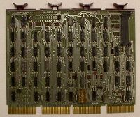
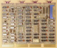
Later versions were the M8290 and M8291 quad format cards, also mounted in an SPC slot. The difference between the two is not yet known. All the card versions are [[program compatible]]. | Later versions were the M8290 and M8291 quad format cards, also mounted in an SPC slot. The difference between the two is not yet known. All the card versions are [[program compatible]]. | ||
| + | <br clear=all> | ||
==Registers== | ==Registers== | ||
| Line 43: | Line 44: | ||
The first buffer register is 12-[[bit]] raw data from the card, the second is the compressed Hollerith code (zones 1-7 can have only a single punch, which is encoded in octal in 3 bits; a '0' means 'no punch in any of these'). | The first buffer register is 12-[[bit]] raw data from the card, the second is the compressed Hollerith code (zones 1-7 can have only a single punch, which is encoded in octal in 3 bits; a '0' means 'no punch in any of these'). | ||
| + | |||
| + | ==External links== | ||
| + | |||
| + | * [http://www.bitsavers.org/pdf/dec/unibus/DEC-11-HCRA-D_CR11_Oct71.pdf CR11 card reader system manual] (DEC-11-HCRA-D) | ||
| + | * [http://www.bitsavers.org/pdf/dec/unibus/DEC-11-HCRB-D_CR11_Mar72.pdf CR11 card reader system manual] (DEC-11-HCRB-D) | ||
| + | * [http://www.bitsavers.org/www.computer.museum.uq.edu.au/pdf/EK-CR11-TM-004%20CR11-CM11%20Card%20Reader%20System%20Manual.pdf CR11/CM11 card reader system manual] (EK-CR11-TM-004) | ||
| + | * [http://www.bitsavers.org/pdf/dec/unibus/CR11_EngrDrws.pdf CR11 card reader engineering drawings] | ||
[[Category:UNIBUS Peripherals]] | [[Category:UNIBUS Peripherals]] | ||
Latest revision as of 00:25, 3 November 2022
The CR11 Controller was a UNIBUS device controller for the CR11 Card Readers. It could also be used with the GDI 100M Optical Mark Reader, which read 12-row 40-column marked cards; in such use, the complete sub-system was called the CM11 Card Reader System.
The CR11 used programmed I/O.
The original version was the M829, a dual format card, which was mounted in an SPC slot; it was used with an M105 Address Selector and an M782 Interrupt Control (both tall singles).
Later versions were the M8290 and M8291 quad format cards, also mounted in an SPC slot. The difference between the two is not yet known. All the card versions are program compatible.
Contents
Registers
The device has three control and buffer registers, which can be configured to any three sequential word locations in the I/O page; it is normally configured to addresses 777160-777164:
| Register | Abbreviation | Address |
|---|---|---|
| Status Register | CRS | 777160 |
| Data Buffer Register | CRB1 | 777162 |
| Data Buffer Register Encoded Output | CRB2 | 777164 |
In the register contents (below), bits which are read/write or unused are shown in normal font, those which are read-only are in italics, and write-only in bold.
Status Register (CRS)
| ERR | CARD DONE | SUPP ERR | RDR CHECK | TIM ERR | RDR ONL | BUSY | RDR RDY | COL RDY | INT ENB | Unused | EJECT | READ | |||
| 15 | 14 | 13 | 12 | 11 | 10 | 09 | 08 | 07 | 06 | 05 | 04 | 03 | 02 | 01 | 00 |
Data Buffer Register (CRB1)
| Unused | Zones 12-10 | Zones 1-9 | |||||||||||||
| 15 | 14 | 13 | 12 | 11 | 10 | 09 | 08 | 07 | 06 | 05 | 04 | 03 | 02 | 01 | 00 |
Data Buffer Register - Encoded Output (CRB2)
| Unused | Zones 12-8 | Encoded Zones 1-7 | |||||||||||||
| 15 | 14 | 13 | 12 | 11 | 10 | 09 | 08 | 07 | 06 | 05 | 04 | 03 | 02 | 01 | 00 |
The first buffer register is 12-bit raw data from the card, the second is the compressed Hollerith code (zones 1-7 can have only a single punch, which is encoded in octal in 3 bits; a '0' means 'no punch in any of these').
External links
- CR11 card reader system manual (DEC-11-HCRA-D)
- CR11 card reader system manual (DEC-11-HCRB-D)
- CR11/CM11 card reader system manual (EK-CR11-TM-004)
- CR11 card reader engineering drawings

