Difference between revisions of "DRV11 Parallel Line Unit"
(basically the same as a DR11-C) |
m (img nm) |
||
| Line 1: | Line 1: | ||
| − | [[Image:DRV11. | + | [[Image:DRV11.jpg|thumb|200px|right|DRV11 board]] |
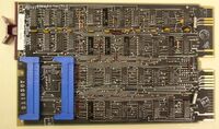
The '''DRV11 Parallel Line Unit''' was a [[QBUS]] [[device controller]] which provided a pair of 16-[[bit]] parallel ports, one input, and one output. It was a [[DEC card form factor|dual]] format card (M7941); it used [[programmed I/O]]. It was fully [[program compatible]] with the [[UNIBUS]] [[DR11-C general device interface]]. | The '''DRV11 Parallel Line Unit''' was a [[QBUS]] [[device controller]] which provided a pair of 16-[[bit]] parallel ports, one input, and one output. It was a [[DEC card form factor|dual]] format card (M7941); it used [[programmed I/O]]. It was fully [[program compatible]] with the [[UNIBUS]] [[DR11-C general device interface]]. | ||
Revision as of 17:25, 10 May 2020
The DRV11 Parallel Line Unit was a QBUS device controller which provided a pair of 16-bit parallel ports, one input, and one output. It was a dual format card (M7941); it used programmed I/O. It was fully program compatible with the UNIBUS DR11-C general device interface.
Connection to the user's device was via a pair of 40-pin Berg connectors. Data going out to the user's device was latched in the DRV11, so may be read at leisure; data coming in from the user's device was merely sampled by the DRV11, so must be held until it has been read.
Contents
Registers
The device had three control and buffer registers, which could be configured to any three sequential word locations in the I/O page. The first DRV11 was normally configured to addresses 767770-767774; the second to 767760-767764, the third to 767750-767754, and so on.
| Register | Abbreviation | Address |
|---|---|---|
| Control and Status Register | DRCSR | 767770 |
| Output Buffer Register | DROUTBUF | 767772 |
| Input Buffer Register | DRINBUF | 767774 |
In the register contents (below), bits which are read/write or unused are shown in normal font, those which are read-only are in italics.
Status Register (DRCSR)
| REQ B | Unused | REQ A | INT ENB A | INT ENB B | Unused | CSR1 | CSR0 | ||||||||
| 15 | 14 | 13 | 12 | 11 | 10 | 09 | 08 | 07 | 06 | 05 | 04 | 03 | 02 | 01 | 00 |
- REQ B - Request B - Signal from user's hardware which can be tested, or cause an interrupt (below)
- REQ A - Request A
- INT ENB A - Interrupt Enable A - When set, allows setting REQ A to cause an interrupt
- INT ENB B - Interrupt Enable B
- CSR1 - Signal to user's hardware (on connector 1)
- CSR0 - Signal to user's hardware (on connector 2)
Output Buffer Register (DROUTBUF)
| OUT15 <-> OUT0 | |||||||||||||||
| 15 | 14 | 13 | 12 | 11 | 10 | 09 | 08 | 07 | 06 | 05 | 04 | 03 | 02 | 01 | 00 |
Input Buffer Register (INBUF)
| IN15 <-> IN0 | |||||||||||||||
| 15 | 14 | 13 | 12 | 11 | 10 | 09 | 08 | 07 | 06 | 05 | 04 | 03 | 02 | 01 | 00 |
