Difference between revisions of "CR11 Controller"
From Computer History Wiki
(Fairly complete) |
(Add image) |
||
| Line 1: | Line 1: | ||
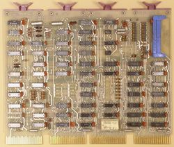
| − | The '''CR11 Controller''' was a [[UNIBUS]] [[device controller]] for the [[CR11 Card Readers]]. It was a [[DEC card form factor|quad]] format card (M8290), and used an [[Small Peripheral Controller|SPC]] slot; it used [[programmed I/O]]. | + | [[Image:CR11-M8291.jpg|thumb|right|250px|M8291 CR11 card]] |
| + | |||
| + | The '''CR11 Controller''' was a [[UNIBUS]] [[device controller]] for the [[CR11 Card Readers]]. It was a [[DEC card form factor|quad]] format card (M8290 or M8291), and used an [[Small Peripheral Controller|SPC]] slot; it used [[programmed I/O]]. | ||
==Registers== | ==Registers== | ||
Revision as of 00:00, 24 January 2019
The CR11 Controller was a UNIBUS device controller for the CR11 Card Readers. It was a quad format card (M8290 or M8291), and used an SPC slot; it used programmed I/O.
Contents
Registers
The device has three control and buffer registers, which can be configured to any three sequential word locations in the I/O page; it is normally configured to addresses 777160-777164:
| Register | Abbreviation | Address |
|---|---|---|
| Status Register | CRS | 777160 |
| Data Buffer Register | CRB1 | 777162 |
| Data Buffer Register Encoded Output | CRB2 | 777164 |
In the register contents (below), bits which are read/write or unused are shown in normal font, those which are read-only are in italics, and write-only in bold.
Status Register (CRS)
| ERR | CARD DONE | SUPP ERR | RDR CHECK | TIM ERR | RDR ONL | BUSY | RDR RDY | COL RDY | INT ENB | Unused | EJECT | READ | |||
| 15 | 14 | 13 | 12 | 11 | 10 | 09 | 08 | 07 | 06 | 05 | 04 | 03 | 02 | 01 | 00 |
Data Buffer Register (CRB1)
| Unused | Zones 12-10 | Zones 1-9 | |||||||||||||
| 15 | 14 | 13 | 12 | 11 | 10 | 09 | 08 | 07 | 06 | 05 | 04 | 03 | 02 | 01 | 00 |
Data Buffer Register - Encoded Output (CRB2)
| Unused | Zones 12-8 | Encoded Zones 1-7 | |||||||||||||
| 15 | 14 | 13 | 12 | 11 | 10 | 09 | 08 | 07 | 06 | 05 | 04 | 03 | 02 | 01 | 00 |
The first buffer register is 12-bit raw data from the card, the second is the compressed Hollerith code (zones 1-7 can have only a single punch, which is encoded in octal in 3 bits; a '0' means 'no punch in any of these').
