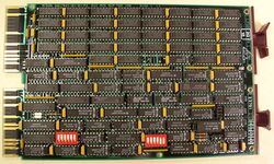
MSV11-M QBUS memory
The MSV11-M (M7506) is a dual-height QBUS DRAM main memory card. The MSV11-MB (M7506-BA) holds 1 MByte when fully populated with 256K DRAMs chips, the MSV11-MA (M7506-AA) is half-populated (the only partially-filled configuration allowed) and holds 512 Kbytes.
The memory is arranged as 2 banks, each 16 data bits (1 PDP-11 word) wide, with 2 additional bits for parity (1 per byte). It is a Q22 card; it reportedly supports QBUS block mode.
Configuration
No documentation on the MSV11-M is extant, so it is currently not known how to configure it. The purpose of the two-position jumper between E19 (apparently a delay line) and E18 is currently unknown.
Control Register
Each board has a single control register, which can be configured in the range 17772100-17772136, using the set of four jumpers between chips E27 and E26. They are not numbered on the board; for our purposes we will number them W1-W4, starting with the left-hand jumper, with the board oriented with the insertion handles at the top.
| W4 | W3 | W2 | W1 | CSR Address |
|---|---|---|---|---|
| In | In | In | In | 17772100 |
| In | In | In | Out | 17772102 |
| In | In | Out | In | 17772104 |
| In | In | Out | Out | 17772106 |
| In | Out | In | In | 17772110 |
| In | Out | In | Out | 17772112 |
| In | Out | Out | In | 17772114 |
| In | Out | Out | Out | 17772116 |
| Out | In | In | In | 17772120 |
| Out | In | In | Out | 17772122 |
| Out | In | Out | In | 17772124 |
| Out | In | Out | Out | 17772126 |
| Out | Out | In | In | 17772130 |
| Out | Out | In | Out | 17772132 |
| Out | Out | Out | In | 17772134 |
| Out | Out | Out | Out | 17772136 |
Technical information
As far as is known, there are no copies of the engineering drawings extant for the MSV11-M.
Further reading
- MSV11-M User Guide (EK-MSV1M-UG - not online)
- MSV11-M Field Maintenance Print Set (MP02053 - not online)
