MSV11-L MOS Random-Access Memory
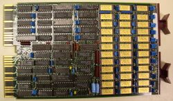
The MSV11-L is a QBUS dual-height DRAM main memory card (M8059). It can be configured as either a Q18 card, or a Q22 card; it supports byte parity.
The memory is arranged as 2 banks, each 16 data bits (one PDP-11 word) wide. The MSV11-LK (M8059-Kx) holds 256 KBytes when fully populated with 64K DRAM chips, the MSV11-LF (M8059-Fx) is half-populated (the only partially-filled configuration allowed) and holds 128 Kbytes. (The 'x' in the board identifier is a capital letter which identifies the manufacturer of the DRAM chips.)
Access time is 210-230 nsec for reads, and 90-120 nsec for writes; cycle times are 560-590 nsec for reads, 605-635 nsec for writes, and 1140-1170 nsec for read/write (DATIO) cycles. Memory refresh time (and conflict delay) is 650-685 nsec.
Contents
Control and Status Register
Each board has a single register, a Control and Status Register, which can be configured in the range 17772100-17772116 (below). In the register contents, all the bits can be read and written by software; all, other than 'Error Address', are cleared by power up and QBUS INIT. Bits which can only be modified by the CPU are shown in normal font, and those which can also be set by the board hardware in italics.
| Parity Error | Extended Error Address Enable | Unused | Error Address | Unused | Write Wrong Parity | Unused | Parity Error Enable | ||||||||
| 15 | 14 | 13 | 12 | 11 | 10 | 09 | 08 | 07 | 06 | 05 | 04 | 03 | 02 | 01 | 00 |
The 'Error Address' field contents depend on the setting of the 'Extended Error Address Enable' bit: when the bit is '0', the field holds the low address (address bits 17 through 11); when the bit is '1', the field holds the high address (address bits 21 through 18 in register bits 8 through 5 - bits 11-9 of the register will still hold address bits 17-15).
Configuration
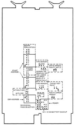
The card is configured by wire-wrap jumpers between posts; it is possible to set:
- the starting address;
- the size (256KB or 128KB);
- the CSR register; and its address, if so;
- parity enable;
- parity error action;
- enable wrong parity;
- bank disable
Since the manual (below) is not available online, here are the jumper details:
| Function | State | Jumper |
|---|---|---|
| Parity | Enable | 9 to 10 |
| Disable | 11 to 10 | |
| Allow clearing 'error enable' | Allow | 20 to 19 |
| Disallow | 18 to 19 | |
| Parity report | BDAL 16 | 3 to 2 |
| BDAL 16 and 17 | 1 to 2 | |
| Write wrong parity | Disable | 8 to 7 |
| Enable | 6 to 7 | |
| CSR | Disable | J to H |
| Enable | F to H | |
| I/O page size | 2KW | 29 to 28 |
| 4KW | 27 to 28 | |
| Board size | Half | 32 to 33 |
| Full | 34 to 33 | |
| Which half | Remove lower | 17 to 16 |
| Normal or Remove upper | 15 to 16 | |
| Q18 or Q22 | Q18 | R to T out |
| Q22 | R to T in |
Register address
Jumper from pin 'E' to the listed pins:
| C | B | A | CSR Address |
|---|---|---|---|
| Out | Out | Out | 17772100 |
| Out | Out | In | 17772102 |
| Out | In | Out | 17772104 |
| Out | In | In | 17772106 |
| In | Out | Out | 17772110 |
| In | Out | In | 17772112 |
| In | In | Out | 17772114 |
| In | In | In | 17772116 |
(Addresses are given in Q22 form; for Q18 operation, delete the high '17'.)
Starting address (high)
Jumper from pin 'K' to the listed pins:
| P | N | M | L | Starting Address |
|---|---|---|---|---|
| Out | Out | Out | Out | 00000000 |
| Out | Out | Out | In | 01000000 |
| Out | Out | In | Out | 02000000 |
| Out | Out | In | In | 03000000 |
| Out | In | Out | Out | 04000000 (1 MB) |
| Out | In | Out | In | 05000000 |
| Out | In | In | Out | 06000000 |
| Out | In | In | In | 07000000 |
| In | Out | Out | Out | 10000000 (2 MB) |
| In | Out | Out | In | 11000000 |
| In | Out | In | Out | 12000000 |
| In | Out | In | In | 13000000 |
| In | In | Out | Out | 14000000 (3 MB) |
| In | In | Out | In | 15000000 |
| In | In | In | Out | 16000000 |
| In | In | In | In | 17000000 |
Starting address (low)
Jumper from pin 'U' to the listed pins:
| Z | Y | X | W | V | Staring Address |
|---|---|---|---|---|---|
| Out | Out | Out | Out | Out | 000000 |
| Out | Out | Out | Out | In | 020000 |
| Out | Out | Out | In | Out | 040000 |
| Out | Out | Out | In | In | 060000 |
| Out | Out | In | Out | Out | 100000 |
| Out | Out | In | Out | In | 120000 |
| Out | Out | In | In | Out | 140000 |
| Out | Out | In | In | In | 160000 |
| Out | In | Out | Out | Out | 200000 |
| Out | In | Out | Out | In | 220000 |
| Out | In | Out | In | Out | 240000 |
| Out | In | Out | In | In | 260000 |
| Out | In | In | Out | Out | 300000 |
| Out | In | In | Out | In | 320000 |
| Out | In | In | In | Out | 340000 |
| Out | In | In | In | In | 360000 |
| In | Out | Out | Out | Out | 400000 |
| In | Out | Out | Out | In | 420000 |
| In | Out | Out | In | Out | 440000 |
| In | Out | Out | In | In | 460000 |
| In | Out | In | Out | Out | 500000 |
| In | Out | In | Out | In | 520000 |
| In | Out | In | In | Out | 540000 |
| In | Out | In | In | In | 560000 |
| In | In | Out | Out | Out | 600000 |
| In | In | Out | Out | In | 620000 |
| In | In | Out | In | Out | 640000 |
| In | In | Out | In | In | 660000 |
| In | In | In | Out | Out | 700000 |
| In | In | In | Out | In | 720000 |
| In | In | In | In | Out | 740000 |
| In | In | In | In | In | 760000 |
Further reading
- MSV11-L User Guide, EK-MSV0L-UG (not available online)
- Differences Between MSVI1-L and MSV11-P Memories, MicroNote #111

