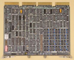
MSV11-R memory module
The MSV11-R (M7458) is a quad-height QBUS/PMI DRAM main memory card.
NOTE: As a PMI card, it uses the CD interconnect; it can therefore only be plugged into a Q/CD backplane. Plugging an MSV11-R card into a regular Q/Q backplane will damage the MSV11-R.
The MSV11-RA (M7358-A) holds 1 MByte when fully populated with 256K DRAM chips. The memory is arranged as 2 banks, each 16 data bits (1 PDP-11 word) wide, with 2 additional bits for parity (1 per byte). In theory, it could support being half-populated (512 Kbytes), with only one bank; there is a jumper, W1, which seems to support this configuration, but no documentation for it. It is not clear if DEC ever sold that configuration.
It is a Q22 card; it also supports block mode (with a maximum block size of 16. words, depending on the block's start address).
Contents
Configuration
A single 8-position DIP switch configures the card:
- Switches S1-S2 sets bits 21-20 of the board's 22-bit starting address;
- DEC documentation asserts that switches S3-S4 must always be off; however they seem to be functional (although perhaps only for the single bank configuration), and set address bits 19-18;
- Switches S5-S8 select the CSR address.
| S1 | S2 | Staring Address |
|---|---|---|
| OFF | OFF | 00000000 (0 MB) |
| OFF | ON | 04000000 (1 MB) |
| ON | OFF | 10000000 (2 MB) |
| ON | ON | 14000000 (3 MB) |
Control Register
Each board has a single control register, which can be configured in the range 17772100-17772136.
| S5 | S6 | S7 | S8 | CSR Address |
|---|---|---|---|---|
| ON | ON | ON | ON | 17772100 |
| ON | ON | ON | OFF | 17772102 |
| ON | ON | OFF | ON | 17772104 |
| ON | ON | OFF | OFF | 17772106 |
| ON | OFF | ON | ON | 17772110 |
| ON | OFF | ON | OFF | 17772112 |
| ON | OFF | OFF | ON | 17772114 |
| ON | OFF | OFF | OFF | 17772116 |
| OFF | ON | ON | ON | 17772120 |
| OFF | ON | ON | OFF | 17772122 |
| OFF | ON | OFF | ON | 17772124 |
| OFF | ON | OFF | OFF | 17772126 |
| OFF | OFF | ON | ON | 17772130 |
| OFF | OFF | ON | OFF | 17772132 |
| OFF | OFF | OFF | ON | 17772134 |
| OFF | OFF | OFF | OFF | 17772136 |
Technical information
A copy of the engineering drawings for the MSV11-R has recently been discovered, in a set of PDP-11/84 engineering drawings (see link below). As described above, each board has 2 banks in the array of DRAM chips; with 256K chips, each bank is thus 512KB. The chips in each bank run across the board (when it is oriented with the chip side facing the viewer, with the metal edging holding the handles at the top). Bit 0 (value 1) of the even byte of the low bank is on the right hand edge of the top row of the array; bit 15 (value 0100000), the top bit of the odd byte, is toward the left hand side of the second row. The two parity bits are on the extreme left hand edge. The high bank is in the third and fourth rows down the board from the metal handle edge. The full bit<->chip table is:
| Bit | Bank 0 | Bank 1 |
|---|---|---|
| 01 | E76 | E78 |
| 02 | E83 | E85 |
| 04 | E90 | E92 |
| 10 | E94 | E96 |
| 20 | E101 | E103 |
| 40 | E108 | E110 |
| 100 | E114 | E116 |
| 200 | E121 | E123 |
| 400 | E75 | E77 |
| 1000 | E82 | E84 |
| 2000 | E89 | E91 |
| 4000 | E93 | E95 |
| 10000 | E100 | E102 |
| 20000 | E107 | E109 |
| 40000 | E113 | E115 |
| 100000 | E120 | E122 |
| Low byte Parity | E128 | E130 |
| High byte Parity | E127 | E129 |
The following 256K DRAM chips have been observed to be used: MB81256-15 (Fujitsu).
Further reading
- MSV11-R User Guide, EK-MSV1R-UG
External links
- 11/84 Field Maintenance Print Set (MP-02015-001) - Contains MSV11-R engineering drawings on pp. 29-45
