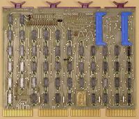
Difference between revisions of "DR11-C general device interface"
m (move to new subcat) |
m (→External links: +manuals, engdrwngs) |
||
| Line 1: | Line 1: | ||
[[Image:DR11-C.jpeg|thumb|200px|right|DR11-C board]] | [[Image:DR11-C.jpeg|thumb|200px|right|DR11-C board]] | ||
| − | The '''DR11-C general device interface''' was a [[UNIBUS]] [[device controller]] which provided a pair of 16-[[bit]] parallel ports, one input, and one output. It was a [[DEC card form factor|quad]] format card (M7860), and used an [[Small Peripheral Controller|SPC]] slot; it used [[programmed I/O]]. | + | The '''DR11-C general device interface''' was a [[UNIBUS]] [[device controller]] which provided a pair of 16-[[bit]] [[parallel interface|parallel ports]], one input, and one output. It was a [[DEC card form factor|quad]] format card (M7860), and used an [[Small Peripheral Controller|SPC]] slot; it used [[programmed I/O]]. |
Connection to the [[user]]'s device is via a pair of 40-[[pin]] [[Berg connector]]s. A pair of optional single-width paddle cards (M971) may be connected via [[flat cable]]s. Data going out to the user's device was latched in the DR11-C, so may be read at leisure; data coming in from the user's device was merely sampled by the DR11-c, so must be held until it has been read. | Connection to the [[user]]'s device is via a pair of 40-[[pin]] [[Berg connector]]s. A pair of optional single-width paddle cards (M971) may be connected via [[flat cable]]s. Data going out to the user's device was latched in the DR11-C, so may be read at leisure; data coming in from the user's device was merely sampled by the DR11-c, so must be held until it has been read. | ||
| Line 44: | Line 44: | ||
| colspan=16 | ''IN15 <-> IN0'' | | colspan=16 | ''IN15 <-> IN0'' | ||
{{16bit-bitout}} | {{16bit-bitout}} | ||
| + | |||
| + | ==External links== | ||
| + | |||
| + | * [http://www.bitsavers.org/www.computer.museum.uq.edu.au/pdf/DEC-11-HDRCA-C-D%20DR11-C%20General%20Device%20Interface%20Manual.pdf DR11-C general device interface manual] (DEC-11-HDRCA-C-D) | ||
| + | * [http://www.bitsavers.org/pdf/dec/unibus/EK-DR11C-TM-004_DR11-C_General_Device_Interface_Manual_Jun74.pdf DR11-C general device interface manual] (EK-DR11C-TM-004) | ||
| + | * [http://www.bitsavers.org/pdf/dec/unibus/DR11-C_EngrDrws.pdf DR11-C general device interface engineering drawings] | ||
[[Category: UNIBUS Parallel Interfaces]] | [[Category: UNIBUS Parallel Interfaces]] | ||
Latest revision as of 23:26, 24 November 2022
The DR11-C general device interface was a UNIBUS device controller which provided a pair of 16-bit parallel ports, one input, and one output. It was a quad format card (M7860), and used an SPC slot; it used programmed I/O.
Connection to the user's device is via a pair of 40-pin Berg connectors. A pair of optional single-width paddle cards (M971) may be connected via flat cables. Data going out to the user's device was latched in the DR11-C, so may be read at leisure; data coming in from the user's device was merely sampled by the DR11-c, so must be held until it has been read.
The DR11-C is the replacement for the earlier multi-board DR11-A General Device Interface. The DR11-C is slightly enhanced over the DR11-A (the -A does not have the CSR1/CSR0 bits).
Contents
Registers
The device has three control and buffer registers, which can be configured to any three sequential word locations in the I/O page; the first DR11-C is normally configured to addresses 767770-767774:
| Register | Abbreviation | Address |
|---|---|---|
| Control and Status Register | DRCSR | 767770 |
| Output Buffer Register | DROUTBUF | 767772 |
| Input Buffer Register | DRINBUF | 767774 |
In the register contents (below), bits which are read/write or unused are shown in normal font, those which are read-only are in italics.
Status Register (DRCSR)
| REQ B | Unused | REQ A | INT ENB A | INT ENB B | Unused | CSR1 | CSR0 | ||||||||
| 15 | 14 | 13 | 12 | 11 | 10 | 09 | 08 | 07 | 06 | 05 | 04 | 03 | 02 | 01 | 00 |
- REQ B - Request B - Signal from user's hardware which can be tested, or cause an interrupt (below)
- REQ A - Request A
- INT ENB A - Interrupt Enable A - When set, allows setting REQ A to cause an interrupt
- INT ENB B - Interrupt Enable B
- CSR1 - Signal to user's hardware (on connector 1)
- CSR0 - Signal to user's hardware (on connector 2)
Output Buffer Register (DROUTBUF)
| OUT15 <-> OUT0 | |||||||||||||||
| 15 | 14 | 13 | 12 | 11 | 10 | 09 | 08 | 07 | 06 | 05 | 04 | 03 | 02 | 01 | 00 |
Input Buffer Register (INBUF)
| IN15 <-> IN0 | |||||||||||||||
| 15 | 14 | 13 | 12 | 11 | 10 | 09 | 08 | 07 | 06 | 05 | 04 | 03 | 02 | 01 | 00 |
External links
- DR11-C general device interface manual (DEC-11-HDRCA-C-D)
- DR11-C general device interface manual (EK-DR11C-TM-004)
- DR11-C general device interface engineering drawings
