Difference between revisions of "PDP-8/I"
(+links, Ext links) |
(MC-8/I details) |
||
| Line 28: | Line 28: | ||
* KA8/IB Positive I/O Bus Interface, to allow use of newer PDP-8 devices | * KA8/IB Positive I/O Bus Interface, to allow use of newer PDP-8 devices | ||
* MC8/I Memory Extension Control, [[bank switching]] needed to support more than 4K [[word]]s of memory | * MC8/I Memory Extension Control, [[bank switching]] needed to support more than 4K [[word]]s of memory | ||
| − | * MP8/I Memory Parity | + | * MP8/I Memory [[Parity]] |
* KE8/I [[Extended Arithmetic Element]], which supported [[hardware]] integer multiplication and division, one-[[bit]] double-word shifts, and [[normalization]] | * KE8/I [[Extended Arithmetic Element]], which supported [[hardware]] integer multiplication and division, one-[[bit]] double-word shifts, and [[normalization]] | ||
* KT8/I Time Sharing Hardware Modification, which allowed the computer to operate in either Executive Mode or User Mode | * KT8/I Time Sharing Hardware Modification, which allowed the computer to operate in either Executive Mode or User Mode | ||
It could perform an addition to the [[accumulator]] in 3.0 μseconds, and a 12 by 12 bit multiplication with 24 bit result in 6.0 μseconds, using the math extension hardware. | It could perform an addition to the [[accumulator]] in 3.0 μseconds, and a 12 by 12 bit multiplication with 24 bit result in 6.0 μseconds, using the math extension hardware. | ||
| + | |||
| + | The MC-8/I had three 3-bit [[register]]s: the Instruction Field and associated Instruction Buffer, and Data Field, which could be loaded either manually from the [[front panel]], or under program control (by the Change Instruction Field - something of a misnomer, as it was actually the IB which was loaded - and Change Data Field [[instruction]]s). The IB contents were loaded into the IF by a [[jump]] or [[subroutine]] call. | ||
==Images== | ==Images== | ||
Revision as of 18:07, 16 May 2021
| PDP-8/I | |
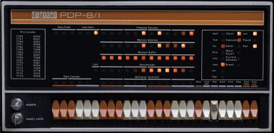
 PDP-8/I front panel | |
| Year Introduced: | 1968 |
|---|---|
| Form Factor: | minicomputer |
| Word Size: | 12 |
| Logic Type: | TTL |
| Design Type: | clocked random logic |
| Clock Speed: | 333KHz |
| Memory Speed: | 1.5 μseconds |
| Physical Address Size: | 32KW (requires optional MC8/I) |
| Virtual Address Size: | 4KW |
| Memory Management: | bank selection, CPU mode |
| Bus Architecture: | negative I/O bus |
| Operating System: | TSS/8. Disk Monitor System |
| Predecessor(s): | PDP-8 |
| Successor(s): | PDP-8/E |
The PDP-8/I was introduced in 1968 as the successor to the PDP-8. It was constructed out of TTL ICs on M-class FLIP CHIPs; the first DEC computer to be built using ICs.
Options included:
- KA8/IB Positive I/O Bus Interface, to allow use of newer PDP-8 devices
- MC8/I Memory Extension Control, bank switching needed to support more than 4K words of memory
- MP8/I Memory Parity
- KE8/I Extended Arithmetic Element, which supported hardware integer multiplication and division, one-bit double-word shifts, and normalization
- KT8/I Time Sharing Hardware Modification, which allowed the computer to operate in either Executive Mode or User Mode
It could perform an addition to the accumulator in 3.0 μseconds, and a 12 by 12 bit multiplication with 24 bit result in 6.0 μseconds, using the math extension hardware.
The MC-8/I had three 3-bit registers: the Instruction Field and associated Instruction Buffer, and Data Field, which could be loaded either manually from the front panel, or under program control (by the Change Instruction Field - something of a misnomer, as it was actually the IB which was loaded - and Change Data Field instructions). The IB contents were loaded into the IF by a jump or subroutine call.
Images
External links
- PDP-8/I - Original PDP-8/I documents
| v • d • e PDP-8 Computers, Software and Peripherals |
|---|
| PDP-8s: PDP-5 • PDP-8 • LINC-8 • PDP-8/S • PDP-8/I • PDP-8/L • PDP-12 • PDP-8/E • PDP-8/F • PDP-8/M • PDP-8/A
Workstations: VT78 Also: PDP-8 family • PDP-8 architecture • PDP-8 Memory Extension units |
