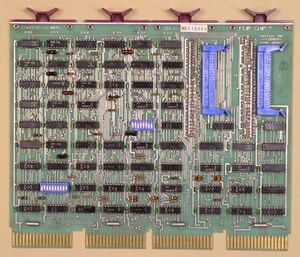
DR11-L general-purpose interface
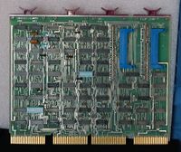
The DR11-L general-purpose interface was a UNIBUS device controller which provided a pair of 16-bit parallel ports, both input-only. It was a quad format card (M7864), and used an SPC slot; it used programmed I/O.
The DR11-L is roughly an input-only version of the earlier DR11-C general device interface, but is not program compatible with the DR11-C.
Connection to the user's device is via a pair of 40-pin Berg connectors; each is controlled by a separate set of registers (identical for the two connectors). Unlike the DR11-C, data coming in from the user's device is latched in the DR11-L, so may be read at leisure.
Contents
Configuration
The device's register and interrupt vector addresses are set by a pair of DIP switches. Unusually for a UNIBUS device, its interrupt priority is also set by the switches. Both the vector and priority may be read in the Control and Status Register.
Registers
The device has two pairs of control and buffer registers, which can be configured to any four sequential word locations in the I/O page; the first DR11-L is normally configured to addresses 764000-76406:
| Register | Abbreviation | Address |
|---|---|---|
| Control and Status Register A | DRCSRA | 764000 |
| Data Buffer Register A | DBDBRA | 764002 |
| Control and Status Register B | DRCSRB | 764004 |
| Data Buffer Register B | DBDBRB | 764006 |
In the register contents (below), bits which are read/write or unused are shown in normal font, those which are read-only are in italics.
Control and Status Register (DRCSR)
| SI | Vector | SO | RQ | RQE | Prority | DR | CID | DL | DAE | ||||||
| 15 | 14 | 13 | 12 | 11 | 10 | 09 | 08 | 07 | 06 | 05 | 04 | 03 | 02 | 01 | 00 |
- SI - Status In: Signal from user's hardware which can be tested
- SO - Status Out: Signal to user's hardware
- RQ - Request: Signal from user's hardware which can be tested, or cause an interrupt
- RQE - Request Enable: Allows setting RQ to cause an interrupt
- DR - Data Ready: Monitors the Data Ready In signal
- CID - CSR ID
- DL - Data Latch: Set by Data Ready In to signal data has been latched
- DAE - Data Accepted Enable: Enables Data Accepted Out to user's hardware
Data Buffer Register (DRDBR)
| IN15 <-> IN0 | |||||||||||||||
| 15 | 14 | 13 | 12 | 11 | 10 | 09 | 08 | 07 | 06 | 05 | 04 | 03 | 02 | 01 | 00 |
Further reading
- DR11-L/M User Manual (EK-DR11L-OP) - not online
- DR11-L Field Maintenance Print Set (MP00003) - not online

