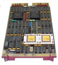
KDJ11-A CPU
The KDJ11-A CPU board (M8192) is the first QBUS PDP-11 CPU card using the J-11 chip set. It is a dual-height board, and was used to upgrade PDP-11/23 systems. (Confusingly, no DEC 'PDP-11/xx' system is specified as using the KDJ11-A.)
It contains an 8K-byte write-through cache (set size 1, block size 1 16-bit word), protected by parity; cache control logic inspects DMA transfers on the QBUS and invalidates cache entries for main memory which is written to by a device.
It also provides a set of diagnostic LEDs, and a line time clock; but no other devices (boot PROM, serial line, etc). Both the LTC, and its control register, are enabled by a single configuration jumper (below).
Although the J-11 does implement FP11 floating-point, the board can also use the optional FPJ11 floating point accelerator chip; note that only the -YB version of the board operates correctly with the FPJ11.
Configuration
A limited amount of configuration can be done with a set of nine jumpers (in the middle of the card).Their functions are:
| Jumper | Function | In | Out |
|---|---|---|---|
| W1 | Bootstrap address bit 15 | 1 | 0 |
| W2 | Bootstrap address bit 14 | 1 | 0 |
| W3 | Powerup option bit 2 | ||
| W4 | Bootstrap address bit 13 | 1 | 0 |
| W5 | Halt enable | Halt | Trap to 4 |
| W6 | Bootstrap address bit 12 | 1 | 0 |
| W7 | Powerup option bit 1 | ||
| W8 | Wakeup circuit | Disabled | Enabled |
| W9 | BEVNT/LTC register | Disabled | Enabled |
Powerup options are:
| W3 | W7 | Action |
|---|---|---|
| In | In | PC from 024, PS from 026 |
| In | Out | ODT, PS=0 |
| Out | In | PC=0173000, PS=340 |
| Out | Out | PC=configuration jumpers, PS=340 |
Further reading
External links
- KDJ11-A CPU Module User's Guide (EK-KDJ1A-UG-002)
- KDJ11-A Field Maintenance Print Set (MP01890-01)
