Difference between revisions of "KTJ11-B UNIBUS adapter"
m (→External links: better cat) |
(Oops, didn't write a complete sentence in the intro) |
||
| (3 intermediate revisions by the same user not shown) | |||
| Line 1: | Line 1: | ||
[[Image:KTJ11-B.jpg|300px|thumb|right|KTJ11-B board]] | [[Image:KTJ11-B.jpg|300px|thumb|right|KTJ11-B board]] | ||
| − | The '''KTJ11-B UNIBUS adaptor''' is used with the [[KDJ11-B CPU|KDJ11-B]] and [[KDJ11-E CPU|KDJ11-E]] [[QBUS]] [[Central Processing Unit|CPU]] cards to add [[UNIBUS]] capability to systems built around those | + | The '''KTJ11-B UNIBUS adaptor''' is used with the [[KDJ11-B CPU|KDJ11-B]] and [[KDJ11-E CPU|KDJ11-E]] [[QBUS]] [[Central Processing Unit|CPU]] cards in the special [[KDJ11 PMI/UNIBUS backplane]] to add [[UNIBUS]] capability to systems built around those cards; the [[PDP-11/84]] and [[PDP-11/94]] systems respectively. It converts the native [[Private Memory Interconnect]] (PMI) [[bus]] supported by these CPUs to the [[Digital Equipment Corporation|DEC]]-standard UNIBUS. |
| − | It is a [[DEC card form factor|hex-height]] board ('''M8191'''), and can only plug into | + | It is a [[DEC card form factor|hex-height]] board ('''M8191'''), and can only plug into the special [[backplane]], unique to those systems, which is wired to support it. |
| − | == | + | ==Technical details== |
| − | The | + | The KTJ11-B contains a [cache]], to increase the efficiency of [[Direct Memory Access|DMA]] transfers on the UNIBUS; generally, two DMA red cycles on the UNIBUS result in a single PMI bus read operation. The cache contains 32 [[word]]-width entries, arranged into 4 independent 8-word sets; the KTJ11-B can thus handle 4 simultaneous DMA operations on the UNIBUS efficiently. |
| − | |||
| − | |||
| − | |||
| − | |||
| − | |||
| − | |||
| − | |||
| − | |||
| − | |||
| − | |||
| − | |||
| − | |||
| − | |||
| − | |||
| − | |||
| − | |||
| − | |||
| − | |||
| − | |||
| − | |||
| − | |||
| − | |||
| − | |||
| − | |||
| − | |||
| − | |||
| − | |||
| − | |||
| − | |||
| − | |||
| − | |||
| − | |||
| − | |||
| − | |||
| − | |||
| − | |||
| − | |||
| − | |||
| − | |||
| − | |||
| − | |||
| − | |||
| − | |||
| − | |||
| − | |||
| − | |||
| − | |||
| − | |||
| − | |||
| − | |||
| − | |||
| − | |||
| − | |||
| − | |||
| − | |||
| − | |||
| − | |||
| − | |||
| − | |||
| − | |||
| − | |||
| − | |||
| − | |||
| − | |||
| − | |||
| − | |||
| − | |||
| − | |||
| − | |||
| − | |||
| − | |||
| − | |||
| − | |||
| − | |||
| − | |||
| − | |||
| − | |||
==External links== | ==External links== | ||
* [http://www.bitsavers.org/pdf/dec/pdp11/1184/EK-1184E-TM-001_Dec87.pdf PDP-11/84 System Technical and Reference Manual] (EK-1184E-TM-001) - the KTJ11-B is covered on pp. 68-85 of the PDF | * [http://www.bitsavers.org/pdf/dec/pdp11/1184/EK-1184E-TM-001_Dec87.pdf PDP-11/84 System Technical and Reference Manual] (EK-1184E-TM-001) - the KTJ11-B is covered on pp. 68-85 of the PDF | ||
| + | * [http://www.bitsavers.org/pdf/dec/pdp11/handbooks/PDP-11_Systems_Handbook_1987.pdf PDP-11 Systems Handbook] (EB 29317 41) - the KTJ11-B is covered on pp. 143-147 of the PDF | ||
* [http://www.bitsavers.org/pdf/dec/pdp11/1184/MP-02015-01_11-84_Maintenance_Print_Set_198412.pdf 11/84 Field Maintenance Print Set (MP-02015-001)] - Contains KTJ11-B Field Maintenance Print Set (MP-02010-01) on pp. 127-156 | * [http://www.bitsavers.org/pdf/dec/pdp11/1184/MP-02015-01_11-84_Maintenance_Print_Set_198412.pdf 11/84 Field Maintenance Print Set (MP-02015-001)] - Contains KTJ11-B Field Maintenance Print Set (MP-02010-01) on pp. 127-156 | ||
[[Category: PDP-11 UNIBUS Processors]] | [[Category: PDP-11 UNIBUS Processors]] | ||
[[Category: UNIBUS]] | [[Category: UNIBUS]] | ||
| + | [[Category: Private Memory Interconnect]] | ||
Latest revision as of 01:07, 8 October 2024
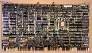
The KTJ11-B UNIBUS adaptor is used with the KDJ11-B and KDJ11-E QBUS CPU cards in the special KDJ11 PMI/UNIBUS backplane to add UNIBUS capability to systems built around those cards; the PDP-11/84 and PDP-11/94 systems respectively. It converts the native Private Memory Interconnect (PMI) bus supported by these CPUs to the DEC-standard UNIBUS.
It is a hex-height board (M8191), and can only plug into the special backplane, unique to those systems, which is wired to support it.
Technical details
The KTJ11-B contains a [cache]], to increase the efficiency of DMA transfers on the UNIBUS; generally, two DMA red cycles on the UNIBUS result in a single PMI bus read operation. The cache contains 32 word-width entries, arranged into 4 independent 8-word sets; the KTJ11-B can thus handle 4 simultaneous DMA operations on the UNIBUS efficiently.
External links
- PDP-11/84 System Technical and Reference Manual (EK-1184E-TM-001) - the KTJ11-B is covered on pp. 68-85 of the PDF
- PDP-11 Systems Handbook (EB 29317 41) - the KTJ11-B is covered on pp. 143-147 of the PDF
- 11/84 Field Maintenance Print Set (MP-02015-001) - Contains KTJ11-B Field Maintenance Print Set (MP-02010-01) on pp. 127-156
