Difference between revisions of "KI10"
(→Busses: KA10-style memories require use of a KI10-M Memory Bus Adapter) |
m (→External links: +one from Paul Allen's collection at the LCM) |
||
| Line 38: | Line 38: | ||
The KI10 Memory Bus is slightly different from that of the [[KA10]]; KA10-style memories can be used on a KI10, but require use of a [[KI10-M Memory Bus Adapter]] (see Section 6.7 of the KI10 Central Processor Maintenance Manual). | The KI10 Memory Bus is slightly different from that of the [[KA10]]; KA10-style memories can be used on a KI10, but require use of a [[KI10-M Memory Bus Adapter]] (see Section 6.7 of the KI10 Central Processor Maintenance Manual). | ||
| + | <br clear=all> | ||
==External links== | ==External links== | ||
| Line 45: | Line 46: | ||
* [http://www.bitsavers.org/pdf/dec/modules/KI10_moduleSchems_V1_Oct74.pdf PDP-10 module schematics Vol.1] | * [http://www.bitsavers.org/pdf/dec/modules/KI10_moduleSchems_V1_Oct74.pdf PDP-10 module schematics Vol.1] | ||
* [http://www.bitsavers.org/pdf/dec/modules/KI10_moduleSchems_V2_Oct74.pdf PDP-10 module schematics Vol.2] | * [http://www.bitsavers.org/pdf/dec/modules/KI10_moduleSchems_V2_Oct74.pdf PDP-10 module schematics Vol.2] | ||
| + | * [https://onlineonly.christies.com/s/firsts-history-computing-paul-g-allen-collection/dec-pdp-10-ki10-mainframe-computer-125/230064?ldp_breadcrumb=back DEC PDP-10 KI10 mainframe computer] - one from [[Paul Allen]]'s collection at the [[Living Computer Museum|LCM]], includes several images | ||
[[Category: PDP-10 Processors]] | [[Category: PDP-10 Processors]] | ||
Revision as of 12:53, 22 April 2025
| KI10 | |
| Manufacturer: | Digital Equipment Corporation |
|---|---|
| Architecture: | PDP-10 |
| Year Design Started: | December, 1969 |
| Year First Shipped: | May, 1972 |
| Form Factor: | mainframe |
| Word Size: | 36 bits |
| Logic Type: | TTL ICs |
| Design Type: | clocked synchronous |
| Instruction Speed: | 1 μsec |
| Memory Speed: | 1.0 μsec (fast), 1.8 μsec (slow) |
| Physical Address Size: | 22 bits |
| Virtual Address Size: | 18 bits |
| Memory Management: | paging, 512-word pages |
| Operating System: | TOPS-10, TENEX, TYMCOM-X |
| Predecessor(s): | KA10 |
| Successor(s): | KL10 |
| Price: | US$200K (CPU), US$500K-1M (system) |
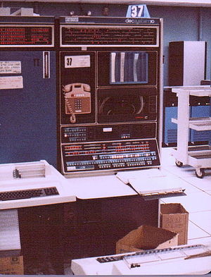
The KI10 was the second generation of PDP-10 processors (themselves, exact re-implementations of the earlier PDP-6 architecture). It was built out of TTL chips, on small FLIP CHIP cards.
It was the first PDP-10 model to provide paging in its as-shipped form, with 512-word pages. It was initially released in a single-CPU version (DECsystem-1060 and -1070); a two-CPU version (DECsystem-1077) was released later.
It was used in later DECsystem-10 models, running TOPS-10. Via a series of kludges, it was also possible to run TENEX on the as-shipped hardware.
A few documents refer to the KI10-based system as PDP-10I.
Busses
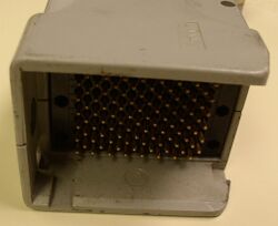
Although the KI10 CPU provided two each of PDP-10 Memory Bus and PDP-10 I/O Bus connectors (Quick Latch connectors for the former), there is only one bus of each type; the two connectors are provided for physical cabling convenience (left and right of the CPU cabinet).
The KI10 Memory Bus is slightly different from that of the KA10; KA10-style memories can be used on a KI10, but require use of a KI10-M Memory Bus Adapter (see Section 6.7 of the KI10 Central Processor Maintenance Manual).
External links
- BitSavers KI10 documents
- PDP-10 module schematics Vol.1
- PDP-10 module schematics Vol.2
- DEC PDP-10 KI10 mainframe computer - one from Paul Allen's collection at the LCM, includes several images

