Difference between revisions of "PDP-10 Memory Bus"
(Redirect for now, pending close of debate) |
(Make into separate page) |
||
| Line 1: | Line 1: | ||
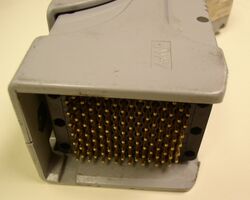
| − | + | [[Image:KBusQCLatched.jpg|250px|thumb|right|Memory bus Quick Latch connector (in latched position)]] | |
| + | |||
| + | The '''PDP-10 Memory Bus''', the [[main memory]] [[bus]] of the [[PDP-10]], existed in three generations. (There were likewise three generations of [[PDP-10 memories|memory systems]] to attach to them.) | ||
| + | |||
| + | The first two were the so-called 'external memory bus', in KA (18-bit [[address]]) and KI (22-bit) forms (for the [[KA10]], and [[KI10]] and early [[KL10]], respectively), although they also had minor [[protocol]] differences. | ||
| + | |||
| + | The last was the 'internal memory bus', the '''S-Bus'''. (For the later KL10s, a later version of the S-Bus, the '''X-Bus''', differed only in the [[logic family]] it interfaced to). | ||
| + | |||
| + | The differences between the two external bus types required a [[KI10-M Memory Bus Adapter]] if KA-type units were to be attached to a KI10. Similarly, KI-type units could be attached to the S-Bus using a [[DMA20 Memory Bus Adapter]]. | ||
| + | |||
| + | For [[Direct Memory Access|DMA]], [[mass storage]] peripherals connected directly to memories (PDP-10 memories are generally [[multi-port memory|multi-port]]). | ||
| + | |||
| + | ==Physical form== | ||
| + | |||
| + | On the KA10, all the busses were physically instantiated as cables with a pair of [[DEC card form factor|dual]] width [[printed circuit board|PCBs]] at each end, which plugged into slots in a standard DEC [[backplane]]; these later became the CJ connectors. | ||
| + | |||
| + | On the KI10, and KL10s with an external memory bus, the memory bus cables ended in a large QuickLatch connector; these connectors were also used on the CPU end of I/O bus cables of those machines. | ||
| + | |||
| + | ==External links== | ||
| + | |||
| + | * [http://www.bitsavers.org/pdf/dec/pdp10/KL10/EK-108OU-PD-002_KL10-Based_Physical_Description_Mar77.pdf EK-108OU-PD-002], "KL10-Based Physical Description" - has images of CJ dual card connectors and QuickLatch connectors, pp. 69-70 | ||
| + | |||
| + | [[Category: PDP-10s]] | ||
Revision as of 03:22, 23 October 2022
The PDP-10 Memory Bus, the main memory bus of the PDP-10, existed in three generations. (There were likewise three generations of memory systems to attach to them.)
The first two were the so-called 'external memory bus', in KA (18-bit address) and KI (22-bit) forms (for the KA10, and KI10 and early KL10, respectively), although they also had minor protocol differences.
The last was the 'internal memory bus', the S-Bus. (For the later KL10s, a later version of the S-Bus, the X-Bus, differed only in the logic family it interfaced to).
The differences between the two external bus types required a KI10-M Memory Bus Adapter if KA-type units were to be attached to a KI10. Similarly, KI-type units could be attached to the S-Bus using a DMA20 Memory Bus Adapter.
For DMA, mass storage peripherals connected directly to memories (PDP-10 memories are generally multi-port).
Physical form
On the KA10, all the busses were physically instantiated as cables with a pair of dual width PCBs at each end, which plugged into slots in a standard DEC backplane; these later became the CJ connectors.
On the KI10, and KL10s with an external memory bus, the memory bus cables ended in a large QuickLatch connector; these connectors were also used on the CPU end of I/O bus cables of those machines.
External links
- EK-108OU-PD-002, "KL10-Based Physical Description" - has images of CJ dual card connectors and QuickLatch connectors, pp. 69-70
