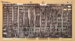
KK11-A Cache Memory
The KK11-A Cache Memory was an option for the KD11-EA CPU, one which added a high-speed cache to the CPU.
Physically, it was a single hex board, the M8268, interfaced to the CPU through an 'over the back' connector. (This was likely because the PDP-11/34 could be field-upgraded from a KD11-E CPU, which did not support the cache, to a KD11-EA, which did - but the original DD11-P backplane was retained.)
Contents
Technical detail
The KK11-A contained 1024 cache entries of high-speed DRAM, in the form of 28 1024x1 DRAM chips. The cache was a direct-mapped cache (i.e. there was only one possible cache entry in which any given word of main memory could be found), with write-through, and a block size of one word.
Each cache entry was 28 bits wide, containing two data bytes; a tag field for cache entries, 7 bits wide (covering UNIBUS address bits 17-11); 3 parity bits (one for the tag); and two valid bits (to allow the entire cache to be cleared by switching to a previously cleared set of valid bits).
Installation
This is mostly covered here, but there is one KK11-A specific detail: a backplane jumper must be present from pin C01E1 to pin B02A1 (the 'cache hit' line).
A check is also required to make sure that the CPU's M8266 card is at the required ECO level - resistor 'R2' must be 1K ohms.
Registers
The cache registers are at the same locations as some of the memory/cache registers in the PDP-11/70, but they are generally incompatible with those in the /70, except as noted below.
| Register | Abbreviation | Address |
|---|---|---|
| Cache Memory Error Register | CME | 777744 |
| Cache Control Register | CCR | 777746 |
| Cache Maintenance Register | CMR | 777750 |
| Cache Hit Register | CHR | 777752 |
In the register contents (below), read-write bits are shown in normal font, read-only in italics, and write-only in bold.
777744: Cache Memory Error Register (CME)
| Unused | High Byte Parity | Low Byte Parity | Tag Parity | Unused | CPU Abort | ||||||||||
| 15 | 14 | 13 | 12 | 11 | 10 | 09 | 08 | 07 | 06 | 05 | 04 | 03 | 02 | 01 | 00 |
Note: The manual says the 'CPU Abort' bit in the CME is bit 1, but the drawings show it as bit 0. Also, no indication is given as to whether these bits are read-only or not; likely they are.
777746: Cache Control Register (CCR)
| Unused | Valid Store In Use | Valid Clear In Progress | Unused | Write Wrong Parity Tag | Unconditional Cache Bypass | Flush Cache | Parity Error Abort | Write Wrong Parity Data | Unused | Force Miss High | Force Miss Low | Unused | Disable Cache Parity Interrupt | ||
| 15 | 14 | 13 | 12 | 11 | 10 | 09 | 08 | 07 | 06 | 05 | 04 | 03 | 02 | 01 | 00 |
777750: Cache Maintenance Register (CMR)
| Unused | Write Tag All Ones | ||||||||||||||
| 15 | 14 | 13 | 12 | 11 | 10 | 09 | 08 | 07 | 06 | 05 | 04 | 03 | 02 | 01 | 00 |
777752: Cache Hit Register (CHR)
| Tag Address | Unused | Hit Register | |||||||||||||
| 15 | 14 | 13 | 12 | 11 | 10 | 09 | 08 | 07 | 06 | 05 | 04 | 03 | 02 | 01 | 00 |
Bit 0 refers to the most recent memory cycle. This field is the only one in the entire register set which is compatible with the -11/70.
External links
- KK11-A cache memory user's guide (EK-KK11A-UG-001)
- KK11-A Field Maintenance Print Set (MP00574)
