KD11-EA CPU
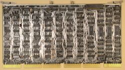
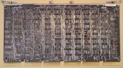
The KD11-EA CPU was the CPU for the PDP-11/34A version of the PDP-11/34; it consisted of two hex printed circuit boards, the M8265 Data Paths module and the M8266 Control module.
The KD11-EA also supported the optional FP11-A floating point (FP11 floating point type) unit and/or the KK11-A cache (it could work with either, or both).
The microcode address space was increased by one bit in the KD11-EA over the KD11-E CPU, to support the extra microcode needed for the floating point instructions.
Contents
Implementation
The implementation was much the same as that of the KD11-E, except that the 512x4 PROMs of the KD11-E were replaced by 1024x4 chips:
| Chip | DEC part number | Bits | Function |
|---|---|---|---|
| E97 | 23-022F1 | 24-27 | B, BX, OVX CTL |
| E98 | 23-023F1 | 28-31 | SSMUX CTL, AMUX CTL |
| E99 | 23-021F1 | 20-23 | FUNC CODE 01-03 |
| E100 | 23-024F1 | 32-35 | ROM SPA 00-03 |
| E103 | 23-011F1 | 40-43 | FORCE K, BUT SERV, PREV, FORCE RSV1 |
| E104 | 23-025F1 | 36-39 | SPA SRC SEL0-1, SPA DST SEL0-1 |
| E105 | 23-019A9/23-027F1 | 44-47 | BUT BITS |
| E106 | 23-020F1 | 16-19 | LOAD BA, LONG CYC, AUX SETUP, FUNC CODE 04 |
| E107 | 23-019F1 | 12-15 | BUF DAT TRAN, BUF C0/C1, ENAB MAINT |
| E108 | 23-018F1 | 8-11 | MPC00, Misc Control |
| E109 | 23-017F1 | 4-7 | MPC01-04 |
| E110 | 23-016F1 | 0-3 | MPC05-08 |
There were also minor changes (mostly chip numbering) to the Instruction Decoder PROMs:
| Chip | DEC part number | Size | Function |
|---|---|---|---|
| E53 | 23-175A2 | 256x4 | Trap Decoder |
| E54 | 23-162A2 | 256x4 | Reset/Trap Decode |
| E59 | 23-174A2 | 256x4 | SOP Decode |
| E60 | 23-173A2 | 256x4 | SOP Microbranch |
| E61 | 23-161A2 | 256x4 | SOP ALU Control |
| E62 | 23-170A2 | 256x4 | Rotate/Shift ALU Control |
| E63 | 23-176A2 | 256x4 | Op Branch |
| E68 | 23-014A9 | 512x4 | Condition Codes |
| E69 | 23-172A2 | 256x4 | DOP Decoder |
| E70 | 23-349A9 | 512x4 | DOP Decoder |
| E72 | 23-A22A2 | 256x4 | Branch Decoder |
| E74 | 23-110A1 | 32x8 | EIS Decoder |
| E83 | 23-107A1 | 32x8 | DOP ALU Control |
The second 'DOP Decoder' chip is the only one which is actually different.
FP11-A/KK11-A installation
Adding either the FP11-A or KK11-A is fairly simple (provided there is adequate power available); they are plugged into the CPU's DD11-P backplane in the slot next to the two CPU boards, and special over the top (OTT) connectors in the form of small PCB cards bearing Berg connectors plug into Berg headers on the two neighbouring cards to connect them up.
(It is not clear why DEC adopted a design which used the OTT cards, although avoiding them would have required the more-expensive upgrade path of a new backplane; there may also not have been enough spare pins on the edge connectors.)
The KK11-A needs only an H8821 two-connector OTT card (40-pin connectors, although the ones used in the H8821 also have 2 blank pins on each end, i.e. the physical form is that of a 44-pin), which goes from the KK11-A to the M8265 card of the CPU.
The FP11-A needs both an H8821, and also the smaller 54-12416 two-connector OTT card, which goes from the M8266 card of the CPU to the FP11-A (28-pin connectors, although 2 pins on each end, and 4 in the centre, are blocked off).
If both an FP11-A and a KK11-A are plugged in, things become slightly more complex. The FP11-A has to be mounted in the slot next to the CPU boards, and the KK11-A has to be mounted in the second slot up from that one.
(The M7859 card for the KY11-LB Programmer's Console is mounted in the slot in the middle; as far as is known, there is nothing special about that slot, and the KY11-LB card could just have been moved over one slot, but DEC must have decided that the documentation would be simpler if it were always in the same slot.)
Instead of the two-connector H8821 OTT card, the very similar H8822 OTT card, with three connectors, must be used instead.
KY11-LB Interface
Like the KD11-E, it also supported the KY11-LB Programmer's Console, including the diagnostic functionality which allowed the CPU's microcode to be single-stepped. The KD11-EA uses the same KY11-L to CPU interface as the other machines that use them.
The interface to the KY11-LB was carried over two 10-wire flat cables connected to Berg connector headers (denominated J1 and J2) on the M8266 module. The pinout for P1 is the same as for the KD11-E; P2 has additional signals (other than μPC08) added in the KD11-EA, though:
J2:
- Micro-PC 08
- FP11-A Attached
- Unused
- Unused
- Unused
- Micro-PC 09
- Service Br Power Fail
- Load Instruction Register
- Power Fail Br Pending
- Unused
No-SACK Timeout Circuitry
In the KD11-EA, the 'No-SACK timeout circuit' was moved from the optional M8264 No-SACK Timeout Module to the main CPU (on the M8265 Data Paths module). See Section 4.7.2.4, "No-SACK Timeout Circuitry", of EK-KD1EA-MM for more.
See also
External links
- KD11-EA central processor maintenance manual (EK-KD1EA-MM-001)
- 1134A Field Maintenance Print Set (MP00190) - the microcode 'Flow Diagram' is mostly missing from this copy (see pg. 30 of the PDF); a complete copy of it is in the KD11-E Field Maintenance Print Set, however (they are the same; errors there were exactly replicated in a Flow Diagram in an offline hard-copy of the KD11-EA Field Maintenance Print Set)

