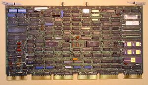
KDF11-U CPU
The KDF11-U is the PDP-11 CPU for the PDP-11/24; it was implemented as a single hex board, the KDF11-UA M7133. It used the same 'Fonz' F-11 chip set as the other KDF11 CPUs; however, it used the UNIBUS, unlike the QBUS of the other KDF11 CPUs. It plugs into a custom slot in the likewise custom PDP-11/24 backplane (DEC part number 54-13817, assembly 70-16905).
The board has seven 40-pin DIP chip sockets for the chipset (including the KTF11-A memory management and KEF11-A floating point chips); it can also hold the double-width KEF11-B 6-chip carrier implementing the PDP-11 Commercial Instruction Set (CIS) (not all KDF11 CPUs can hold this). In addition to the basic CPU functionality, the board also included two asynchronous serial lines (led out through the backplane).
There are two different versions of the KDF11-U; in the later M7133-YA, in order to reduce the cost, a number of individual DIP chips were replaced with a pair of custom gate array chips, and the board was re-laid-out.
The KDF11-U usually operates with the optional UNIBUS map board, the KT24.
Contents
Hardware details
The technical documentation for the KDF11-U is not as complete as it could/should be. Some areas are covered here.
Voltages
The card mostly uses +5 volts, but there is some use of +12V (produced from +15V by the 7812 voltage regulator at top center of page K12 of the KDF11-U Field Maintenance Print Set, 'SC, Interrupt, Voltage Regulation, Front Panel'): CHIP CLK generation (chip E16, top right center of page K1, 'Clock, State Decode'); EIA interface chips (top left corner, page K12); F-11 chips (center of left side, page K13 of the prints, 'Fonz Chips'). There is also minimal use of -12V (produced from -15V at top center of page K12): UART chips (top left corner, page K8, 'SLU 1, Baud', and page K9, 'Address Decode, MIB Buffer, SLU 2'); EIA interface chips (top left corner, page K12).
CPU clock
The CPU's main internal clock is a simple adjustable R/C circuit (in the lower middle of page K1); the trim potentiometer that's part of it is physically just to the left of centre on the very upper edge of the board, and can be adjusted to set the clock speed 'properly'. See the note in the bottom left corner of page K14 ('Switches, Jumpers, Clock Setting' for the adjustment procedure (the clock should be 300 nsec). (The 2.7648 MHz crystal along the upper edge, just to its right, actually drives the baud rate generator for the built-in serial lines.)
Section 4.2 ("Timimg") of the PDP-11/24 Technical Manual (below) covers all the various clocks used by the CPU section of the KDF11-U in some detail.
LED's
The board contains three LED's (along the upper edge), which provide diagnostic information. One (marked 'CLK') an indication that the CPU's main internal clock (on page K1 of the prints, in the very upper left corner) is running. The other two ('0' and '1'; left center, page K12) are driven by a write-only register, and are used by diagnostic code in the bootstrap to indicate progress.
The CLK LED is driven directly by the MCLK L internal signal; if that LED is not on, the CPU is not running. If either the bus ACLO or DCLO signals is asserted, MCLK L is off.
ECO's
Although there's a page in the FMPS (below) which lists ECO's (pg. 167 of the PDF, two pages after K14), there's at least one major ECO which doesn't seem to be listed there. It seems to be a common ECO, though; most KDF11-U's seem to have it. It apparently substituted a transceiver DS8641 gate at E52 (on page K6) for the receiver E70 (also on K6) connected to bus line 'AC LO', so that the KDF11-U could also drive AC LO.
It starts with a cut of the short trace from E70p1 to the plated-through hole (PTH) next to it. A wire is then run from the PTH to E52p4 (the bus line on the transceiver), thereby connecting the latter directly to UNIBUS AC LO (on pin BF1).
E52p5 (the transceiver's input) is connected to E73p13 (an DS8640 quad NOR used as a bus reciver), in the upper left corner of K2. That produces UNIBUS PB L NOR UNIBUS PA H - i.e. a parity error has been detected in memory - to which the response is apparently to power-fail the system!
The incoming ACLO from the transceiver (E52p6) now has a wire going to a PTH next to E70p8. On the bottom side of the PCB, there's a trace from that PTH to E66p13 - which is the inverter (shown on K2) which converts BUF ACLO H to POWER OK H. So that answers the inevitable query about E70p1 (and its output, E70p2) being left floating after the etch cut: perhaps there's an etch cut somewhere that disconnected E66p13 from E70p2, so the former can now be driven by E52p6. (There is a trace from that latter PTH which dives under E70, and although it's hard to see it, it looks like it goes to E70p2.) It would be interesting to know what they did about the E70p2 -> E66p13 connection.
See also
External links
- PDP-11/24 System Technical Manual (EK-11024-TM-001) - the KDF11-U is covered in Chapters 3-5
- PDP-11/24 System Technical Manual (EK-11024-TM-003) - the M7133-YA is documented in Appendix D
- 11/24 Field Maintenance Print Set - KDF11-UA Field Maintenance Print Set (MP01028) is on pp. 145-167
