KA11 CPU

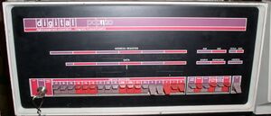
The KA11 is the CPU of the PDP-11/20, the first PDP-11. It was the only PDP-11 CPU which was not microcoded (since the cheap ROMs which make micro-programming cost-effective in smaller machines were not available at the time it was designed).
The KA11 was implemented as a set of extended length FLIP CHIPs, containing early 74 series TTL chips. They all plugged into a custom backplane, formed from three 4-slot system units wired together into one monolithic unit.
Contents
Internal structure
The KA11 is basically divided into four main sections:
- Bus Interface
- Data Paths
- Registers
- Control
(There is also a Console section, which allows the machine's front console to control the CPU, but it is not involved in 'normal' machine operation.)
The Bus Interface and Control sections communicate with the machine's main bus, the UNIBUS; only the former transfers data, the latter's connection is to allow the KA11 to serve as the 'bus arbitrator' for the UNIBUS. Only the Data Paths section can pass data to the Bus Interface section.
There is a 16x16 register file, of which half are used to hold the machine's general registers; two of the others are used for internal temporary registers (Temp and Source). A number of other internal registers (e.g. the Instruction Register and Bus Address Register) are implemented separately, to make them always available. The Register section communicates only with the Data Path section.
The condition codes are part of the Control section, but are generated in the Data Paths section.
State machine
As noted above, the KA11 does not have microcode; instead, it uses a state machine to control the operation of the CPU. There are 5 major states:
- Fetch - obtain and decode the instruction;
- Source - decode the source field of a double-operand instruction, fetch the data, and store it in a temporary;
- Destination - decode the destination field, and obtain the data;
- Execute - use the data obtained in previous states to perform the requested operation, including writing data back to the destination;
- Service - perform special operations such as interrupts, traps, etc.
Each major state contains a number of minor states, as needed to perform the operations of that state (e.g. perform a bus cycle to fetch a memory word). These minor states are named ISRn (from Instruction Shift Register) for minor states associated with internal processor actions, and BSRn (from Bus Shift Register) for minor states associated with bus operations.
Not all instructions pass through all 5 major states, although all do pass through 'Fetch'. 'Source' and 'Destination' are not entered if the mode for that operand is 'Register'; only 'full' double-operand instructions (i.e. those with non-zero mode bits in the source) will enter 'Source' state.
'Source' and 'Destination' are very similar, but within each, the sequence of minor states varies considerably between each of the seven operand modes other than mode 0, direct register access (for which, as previously mentioned, the Source or Destination major state is bypassed entirely).
Data paths
The ALU in the KA11 is an extremely simple one, unlike all other -11's; it can only perform additions.
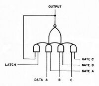
Each input to the adder has a three-input mux (implemented as a NOR gate of three inputs with NANDs to enable them; shown to the side); a latch formed with the output of the mux can also be fed back through the mux (i.e. as a fourth input to it). The A mux can select from register data, and complemented register and bus data; the B mux can select register and bus data.
Enabling two inputs to a mux ORs together the data in the two inputs. To perform an AND, De Morgan's theorem is used; the complemented data inputs are ORed together, and the result is again complemented; this, however, requires two passes through the ALU.
The complemented inputs on the A mux also allow the creation of constants; e.g. simultaneously selecting 'register' and 'complemented register' creates -1. Control of the gating for bit 0 of the A mux is independent of the gating control for bits 15-1, which allows bit 0 to be set to 0 or 1 as needed, to create the constants -2, +1, etc.
A mux on the output allows one-bit shift/rotate operations (the original PDP-11 instruction set does not support multi-bit shifts), as well as byte swapping; the shift capability is used in other ways as well (e.g. in calculating the destinations of branch instructions, which include a word offset).
Bus interface
The DATIP (read with expected write to follow) UNIBUS cycle, especially useful for core memory (which must write the date back into a location which has just been read) when it is known that a write to a location will follow a read of it, is heavily used by the KA11.
Reads in the Destination major state are done as DATIPs, and when the instruction reaches the Execute major state, a 'DATO#' bus cycle is used to write the data back; this is a special internal form of the DATO cycle which indicates that the address to be written to is already available in the Bus Address Register. (Since calculating the address can be a lengthy process, especially if index words or deferred modes are used, the ability to avoid re-doing that computation is very significant.)
Implementation
As previously mentioned, the CPU consisted of two and a half quad system unit backplanes (the two otherwise-unused slots were SPC slots, available for any peripheral) wire-wrapped into a single unit.
Most of the circuitry was on quad-height boards, but there were some duals, and a few singles. The KA11 board set comprises:
| Board | Function |
|---|---|
| Single | |
| M823 | Codes Data |
| M825 | Power Failure and Control |
| Dual | |
| M224 (two instances) | Data Paths (8 bits; 2 latches, adder) |
| M225 | Registers (16 bits x 16) |
| M821 | Register Control |
| M822 | Flag Control |
| M824 | Priority |
| Quad | |
| M724 | Bus and Console Control |
| M725 | Bus Interface and IR |
| M726 | IR Decode |
| M727 | State Control |
| M728 | Timing and States |
| M820 | Data Path Control |
Board locations (as seen from the board insertion side of the backplane, not the wire-wrap pin side, as is common in DEC documentation) are:
| Connector | ||||||
|---|---|---|---|---|---|---|
| Slot | A | B | C | D | E | F |
| 1 | KY11-A | |||||
| 2 | KM11 | M727 | ||||
| 3 | Power | M823 | M728 | |||
| 4 | M825 | M726 | ||||
| 5 | M724 | |||||
| 6 | M725 | |||||
| 7 | Power | M820 | ||||
| 8 | M224 | M224 | ||||
| 9 | UNIBUS termination | M822 | M821 | |||
| 10 | KW11-L | M824 | M225 | |||
| 11 | Power | SPC | ||||
| 12 | UNIBUS Out | SPC | ||||
See also
External links
- 11/20 - documentation at Bitsavers is here
- KA11 processor manual
- PDP-11/20 engineering drawings - KA11 on pp. 3-58 of the PDF; block diagram on pg. 12
- PDP-11/20 modules - KA11 versions
- Details of Design, KA11 - early memo explaining internal operation
- KA11 Design Critique - a retrospective memo as the machine was going into production
