MJ11 memory system
The MJ11 memory system was a core main memory system for the PDP-11/70. It was 32 bits wide, to interface to the -11/70's Main Memory Bus, and provided byte parity (4 bits/double-word). Read, Write, and Exchange cycles were supported.
It came in two variants, the MJ11-A (which used 32KB core stack modules), and the MJ11-B (which used 64KB modules). Both kinds of modules had to be installed in pairs (since they were 16 bits wide, and the MJ11 dealt in 32-bit words).
A maximum of eight MJ11 systems could be installed on a single machine, for a maximum of 2MB of memory when using 32KB modules, or slightly less than 4MB with 64KB modules.
Implementation
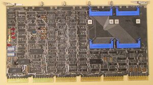
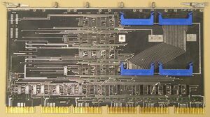
The MJ11 was housed in a BA11-K mounting box, and used a custom 26-slot backplane (DEC part number 70-10497), holding a number of hex boards. These included a pair of control boards - an M8149 transceiver board, and either an M8147 or M8148 control and timing board (the M8148 could only be used with 32KB core stack modules, whereas the M8147 could be used with either); the Main Memory Bus was carried on flat cables, which plugged into Berg connector headers on the control cards. Data was stored on between 1 and 4 pairs of core stack sets.
A 32KB core stack set consisted of:
- G114 sense/inhibit module
- G235 X-Y driver
- H217-C core stack
A 64KB set consisted of:
- G116 sense/inhibit module
- G236 X-Y driver
- H224-C core stack
The 32KB stack set contains the same boards as those in the MM11-U core memory; the 64KB stack set contains the same boards as those in the MM11-W core memory.
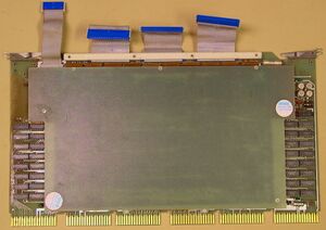
In the 64KB set, the H224-C is connected to the G116/G236 cards with 'over the back' flat cables, which carry the sense/inhibit signals from the core stack board to the electronics board. This is possibly because the MJ11 backplane was designed for use with the MM11-U board set, and changes in the functional modularization may have made those connections unsuitable for use by the 64KB set.
The H224-C core stack is connected to the G236 with a 20-pin cable, and to the G116 with three 40-pin connectors. The cable end on the G116/G236 end is a standard Berg header, but on the H224-C end, the cables are soldered directly to the board, not plugged into a connector.
The stack sets were placed in the backplane from the outer edges (on each side, since they had to be installed in pairs of sets) toward the center; the control boards went in the two center slots. Interestingly, the order within each group of 3 boards was not mirror-imaged; the X-Y driver, core stack, and sense/inhibit module were in the same order on both sides of the center.
Board locations (as seen from the board insertion side of the backplane, not the wire-wrap pin side, as is common in DEC documentation) are:
| Connector | ||||||
|---|---|---|---|---|---|---|
| Slot | A | B | C | D | E | F |
| 1 | G114/G116 sense/inhibit module | |||||
| 2 | H217-C/H224-C core stack | |||||
| 3 | G235/G236 X-Y driver | |||||
| 4-12 | Array sets 1-3 (high half-word) | |||||
| 13 | M8147/M8148 control and timing | |||||
| 14 | M8149 transceiver | |||||
| 15-23 | Array sets 1-3 (low half-word) | |||||
| 24 | G114/G116 sense/inhibit module | |||||
| 25 | H217-C/H224-C core stack | |||||
| 26 | G235/G236 X-Y driver | |||||
Upgrades
An MJ11-A could be upgraded to an MJ11-B by adding a pair of wires to the backplane (presumably for an extra address line), swapping in an M8147 control and timing board for the M8148, and swapping in, or adding, pairs of 64KB board sets. The wire ran from pin EJ1 of the sense/inhibit module to pin EJ2 of the X-Y driver board. (Later backplanes, not just those for the MJ11-B, came with this modification.)
When an MJ11 backplane contained a mix of 32KB and 64KB board sets, the 32KB ones had to be in the lower locations (i.e. the outer edges on each side). Both kinds of sets had to be installed in pairs; i.e. a 32KB set could not be paired with a 64KB set.
See also
Further reading
- MJ11 Memory System Maintenance Manual (EK-MJ11-MM-002) - only available in microfiche
External links
- MJ11 memory system user's manual (EK-MJ11-OP-001)
- MJ11-A Engineering Drawings


