RK11 disk controller
The RK11 and RKV11 series of controllers for the UNIBUS and QBUS are for the earlier RK moving-head magnetic disk drives (RK02-RK05), all based on the IBM 2315 drive and pack.
(The later RK06 and RK07, and their controller, the RK611, are a different and entirely incompatible drive and pack.)
There are several models of the RK11, which are basically identical in their programming interface; differences between them are discussed in the sections on the individual models (below).
The UNIBUS RK11's all connect to the RK drive(s) through a bus carried over a BC11A cable, the standard UNIBUS cable.
Contents
- 1 Early RK11 version
- 2 RK11-C
- 3 RK11-D
- 4 RK11-E
- 5 RKV11-D
- 6 Device registers
- 6.1 777400: Drive Status Register (RKDS)
- 6.2 777402: Error Register (RKER)
- 6.3 777404: Control Status Register (RKCS)
- 6.4 777406: Word Count Register (RKWC)
- 6.5 777410: Current Bus Address Register (RKBA)
- 6.6 777412: Disk Address Register (RKDA)
- 6.7 777414: Maintenance Register (RKMR)
- 6.8 777416: Data Buffer Register (RKDB)
- 7 PDP-11 bootstraps
- 8 External links
- 9 Further reading
Early RK11 version
Although the RK11-C (below) is the earliest documented version, there are a few clues which indicate that there was an earlier version (one for which no documentation remains).
First, there is an image of a DEC indicator panel (image here) which seems to be from a pre-RK11-C; it clearly seems to be an RK11 panel of some sort, but the pinout of the RK11-C indicator panel connector (engineering drawing "RK11-C Indicator Connectors: RK11-C-23") has differences with this one.
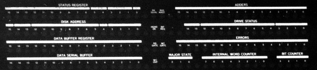
In particular, on the panel in the image, the lower right line of lights on the panel shows 3 bits of Major State; on the RK11-C prints (on connector B32) there are 5 individual bits (Postamble, Checksum, Data, Header, Preamble). To explore this further, on the "Major States" RK11-C drawing (RK11-C-04), in the upper left corner, there is a row of 6 flops, each labeled with one of those states (plus one for 'Idle'), arranged in a chain - the output of each driving an individual light. However, the 3 bits for 'Major State' on the display panel imply it is binary coded - likely implemented with a counter.
Also, the signal "COUNT MSR" (likely 'Major State Register') is exactly what one would expect to see if the major state had previously been held in a counter, not a string of flops. It makes no sense to expend the effort synthesize that signal (on the next page, RK11-C-05, "MSR Control") when the individual signals which go into it could have been used, as is, to clock each flop in the chain.
A reasonable guess, in light of these facts, is that in some previous version, a counter had been used, but had had a problem of some sort, and had therefore been replaced by the string of flops. (The reason is unknown, but perhaps it was a binary counter, not Gray code, and the decoding into states was producing glitches.)
A plausible scenario is that such an earlier version was produced in very small numbers - perhaps as prototypes, only internal to DEC. (If there had been problems discovered with glitches in the major state counter, they would not have wanted to release it as a product.) Or if it was released as a product, perhaps they were all recalled and replaced with RK11-C's.
In this regard, it is interesting to note the DEC Spare Module Handbook, lists only the RK11-C and -D, but does list the KT11-B, a rara avis indeed. This argues that the predecessor did not exist 'in the wild'.
RK11-C
Main article: RK11-C disk controller
Like many of the earlier large peripheral controllers for the PDP-11, the RK11-C was a large custom wire-wrapped backplane which bolts into the front or back of a 19 inch rack, such as an H960; into it were plugged about 40 small M-Series FLIP CHIPs.
The RK11-C supports up to 4 drives per device bus (it uses 4 different 'select' lines on the bus, one of which is asserted at a time), and has two device busses.
RK11-D
The RK11-D was a re-implementation of the RK11-C on four quad cards (M7254-7), which plugged into a custom-wired 4 slot hex-high system unit backplane, for a BA11 slide-out mounting box.
It was program compatible with the RK11-C, except that the RK11-D did not contain the Maintenance Register of the earlier controller. In the RK11-D, the bus location of the MR responds, but according to the engineering drawings, it reads as zero, and written data is ignored.
The RK11-D supports up to 8 drives per device bus (it uses 3 'select' lines on the bus, with the drive number encoded in binary), and has only one device bus.
The RK11-D also has a 6-word FIFO buffer between the disk and the bus (see sheet 7 of the M7256 engineering drawings). The original RK11-C had only one word of buffering, which was probably not enough, and likely the reason for the double-buffered RK11-C version.
RK11-E
The RK11-E (sometimes called the RK15) was a variant of the RK11-D which supported 18-bit data; it was used with the PDP-15. It used the same cards as the RK11-D, with a jumper selection for 18-bit operation, and a different clock crystal.
It was used with the UC15 Unichannel, which used a PDP-11 (usually a PDP-11/05) acting as a slave to the PDP-15; the RK11-E was plugged into the UNIBUS on the PDP-11.
It used the two UNIBUS parity lines for the two extra data bits on the 18-bit PDP-15. The two extra bits were not used by the PDP-11 or its memory, but went straight through the MX15-B Memory Multiplexer, directly to the PDP-15's main memory.
RKV11-D

The RKV11-D is a variant of the RK11-D for the QBUS (the others are all UNIBUS).
It uses three of the four quad cards of the RK11-D (M7254-6), along with a replacement fourth card (M7268), in a different custom 4 slot quad-high system unit backplane. The M7268 is connected via two pairs of flat cables to two dual cards, one of which (M7269) plugs into a QBUS backplane slot, and the other (M993-YA) into the first RK05 drive. The RKV11-D is mounted in a BA11-M style mounting box with H780 power supply. The BA11-M front panel is replaced with an expansion box front panel, with a single indicator for DCOK.
It is program compatible with the RK11-D, except that it only supports Q16 QBUS mode when writing data. The two extended memory bits in the CSR have no effect; they may be read and written, but are not connected to anything.
Device registers
| Register | Abbreviation | Address |
|---|---|---|
| Drive Status Register | RKDS | 777400 |
| Error Register | RKER | 777402 |
| Control Status Register | RKCS | 777404 |
| Word Count Register | RKWC | 777406 |
| Current Bus Address Register | RKBA | 777410 |
| Disk Address Register | RKDA | 777412 |
| Maintenance Register | RKMR | 777414 |
| Data Buffer Register | RKDB | 777416 |
777400: Drive Status Register (RKDS)
| Drive ID | DPL | RK05 | DRU | SIN | SCOK | DRY | R/W/S Ready | WPS | SC=CA | Sector Counter | |||||
| 15 | 14 | 13 | 12 | 11 | 10 | 09 | 08 | 07 | 06 | 05 | 04 | 03 | 02 | 01 | 00 |
Note that in the diagram of this register in the 'peripherals handbook' (both 1975 and 1976 editions), bits 7 and 6 are labelled incorrectly; the table which lists the bits has them correctly.
(To confirm this, consult the RK11-D print set, M7254 page 3; the dual 4->1 muxes which fill this page are the source of the RKDS, RKER, etc registers.)
The name of bit 6 has changed slightly from the RK11-C to the -D ("Access Ready" to "R/W/S Ready"), but it seems to be basically the same functionality.
777402: Error Register (RKER)
| DRE | OVR | WLO | SKE | PGE | NXM | DLT | RTE | NXD | NXC | NXS | CSE | WCE | |||
| 15 | 14 | 13 | 12 | 11 | 10 | 09 | 08 | 07 | 06 | 05 | 04 | 03 | 02 | 01 | 00 |
777404: Control Status Register (RKCS)
| ERR | H.E. | SCP | M | IBA | FMT | R/WA | SSE | RDY | IDE | EX. MEM | FUNCTION | GO | |||
| 15 | 14 | 13 | 12 | 11 | 10 | 09 | 08 | 07 | 06 | 05 | 04 | 03 | 02 | 01 | 00 |
Bit 9 is"Read/Write All" in the RK11-C, and unused in the -D; bit 12 is "Maint" in the -C, and unused in the -D.
| Command | Code | In CSR |
|---|---|---|
| Reset Controller | 0 | 0 |
| Write | 1 | 02 |
| Read | 2 | 04 |
| Write Check | 3 | 06 |
| Seek | 4 | 010 |
| Read Check | 5 | 012 |
| Reset Drive | 6 | 014 |
| Write Lock | 7 | 016 |
777406: Word Count Register (RKWC)
| WC15 <---> WC00 | |||||||||||||||
| 15 | 14 | 13 | 12 | 11 | 10 | 09 | 08 | 07 | 06 | 05 | 04 | 03 | 02 | 01 | 00 |
777410: Current Bus Address Register (RKBA)
| BA15 <---> BA01 | Unused | ||||||||||||||
| 15 | 14 | 13 | 12 | 11 | 10 | 09 | 08 | 07 | 06 | 05 | 04 | 03 | 02 | 01 | 00 |
777412: Disk Address Register (RKDA)
| DRIVE SELECT | CYLINDER ADDRESS | SUR | SECTOR ADDRESS | ||||||||||||
| 15 | 14 | 13 | 12 | 11 | 10 | 09 | 08 | 07 | 06 | 05 | 04 | 03 | 02 | 01 | 00 |
777414: Maintenance Register (RKMR)
| M. RCP | M. RDP | M. SPS | M. ADA | M. LAI | M. DRY | M. R/W/S | MAINT. SECTOR COUNTER | ||||||||
| 15 | 14 | 13 | 12 | 11 | 10 | 09 | 08 | 07 | 06 | 05 | 04 | 03 | 02 | 01 | 00 |
This register is not present in the RK11-D; it reads as 0, and writes to it are discarded.
777416: Data Buffer Register (RKDB)
| DB15 <---> DB00 | |||||||||||||||
| 15 | 14 | 13 | 12 | 11 | 10 | 09 | 08 | 07 | 06 | 05 | 04 | 03 | 02 | 01 | 00 |
PDP-11 bootstraps
Disk 0
| Address | Data | Mnemonic | Description |
|---|---|---|---|
| 1000 | 012700 | MOV #177406,R0 | Move the address of the Word Count register into R0 |
| 1002 | 177406 | (constant) | |
| 1004 | 012710 | MOV #177400,(R0) | Move block size (negative) into Word Count register |
| 1006 | 177400 | (constant) | |
| 1010 | 012740 | MOV #5,-(R0) | Move 'Read Go' command into CSR |
| 1012 | 000005 | (constant) | |
| 1014 | 105710 | TSTB (R0) | Test for 'Done' bit in CSR |
| 1016 | 100376 | BPL 1014 | Jump backward if not set |
| 1020 | 005007 | CLR PC | Start loaded bootstrap with jump to 0 |
Note that the INIT pulse caused by hitting the 'Start' button will clear the Bus Adddress register, so the loaded block will be placed at location 0.
Disk n
This bootstrap will boot from any disk in a daisy-chained multi-drive configuration. Memory location octal 1006 contains the unit number, as follows:
|
|
External links
- RK11-D and RK11-E moving head disk drive controller manual (DEC-11-HRKDA-B-D)
- RK11-D and RK11-E moving head disk drive controller user's manual (EK-RK11D-OP-001)
- RK11-D and RK11-E moving head disk drive controller manual (EK-RK11D-MM-002)
- RKV11-D disk drive controller user's manual (EK-RKV11-0P-001)
- RK11-D disk drive controller engineering drawings (Rev P, 10-1975)
- RK11-D Engineering Drawings (Rev R, 10-1976)
- RK11-D ECOs
Further reading
- RKV11-D disk drive controller technical manual (not available online, but in fiche - EP-RKV11-TM-001)
- RKV11-D Field Maintenance Print Set (MP00223) (not available online)