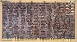
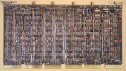
KD11-E CPU
The KD11-E CPU was the first CPU version for the PDP-11/34; it consisted of two hex printed circuit boards, the M7265 Data Paths module and the M7266 Control module. They plugged into a modified MUD backplane, the DD11-P backplane, which was customized for the KD11-E.
Although it supported the KY11-LB Programmer's Console, including the diagnostic functionality which allow the CPU's microcode to be single-stepped, it did not support the FP11-A floating point unit or the KK11-A cache; a PDP-11/34 system needed the upgraded KD11-EA CPU for that.
The KD11-E uses the same KY11-L to CPU interface as the other machines that use them.
Implementation
The KD11-E makes heavy use of PROMs, to hold the microcode, to control the ALU, provide trap addresses, and for instruction decoding. The latter is partially accomplished in microcode, but with extensive assistance from an Instruction Decoder largely implemented in PROMs. The latter has several functional sub-units:
- DOP Decoder, double-operand instructions
- SOP Decoder, single-operand instructions
- Branch Decoder, branch instructions
- Operate Decoder, condition codes instructions
The Instruction Decoder also checks for illegal instructions, and illegal addressing modes on otherwise-legal instructions.
The microcode is 48 bits wide, stored in 12 512x4 PROMs:
| Chip | DEC part number | Bits | Function |
|---|---|---|---|
| E97/E94 | 23-021A9 | 24-27 | B, BX, OVX CTL |
| E98/E95 | 23-022A9 | 28-31 | SSMUX CTL, AMUX CTL |
| E99/E96 | 23-020A9 | 20-23 | FUNC CODE 01-03 |
| E100/E97 | 23-023A9 | 32-35 | BUT BITS |
| E102/E111 | 23-025A9 | 40-43 | FORCE K, BUT SERV, PREV, FORCE RSV1 |
| E103/E112 | 23-024A9 | 36-9 | SPA SRC SEL0-1, SPA DST SEL0-1 |
| E104/E113 | 23-026A9 | 44-47 | ROM SPA 00-03 |
| E105/E114 | 23-019A9 | 16-19 | LOAD BA, LONG CYC, AUX SETUP, FUNC CODE 04 |
| E106/E115 | 23-018A9 | 12-15 | BUF DAT TRAN, BUF C0/C1, ENAB MAINT |
| E107/E116 | 23-017A9 | 8-11 | MPC00, Misc Control |
| E108/E117 | 23-016A9 | 4-7 | MPC01-04 |
| E109/E118 | 23-015A9 | 0-3 | MPC05-08 |
Note: The chip numbers in the KD11-E FMPS (MP0004) are given with two differing assignments; the 'Control Word' diagram (pg. 1 of the 'KD11-E Flow Diagrams') gives one set of numbers (the second, in the table above); the actual prints of the M7266 use another (given as the first in the table above).
Instruction Decoder uses 13 PROMs, of differing sizes:
| Chip | DEC part number | Size | Function |
|---|---|---|---|
| E52 | 23-175A2 | 256x4 | Trap Decoder |
| E53 | 23-162A2 | 256x4 | Reset/Trap Decode |
| E58 | 23-174A2 | 256x4 | SOP Decode |
| E59 | 23-173A2 | 256x4 | SOP Microbranch |
| E60 | 23-161A2 | 256x4 | SOP ALU Control |
| E61 | 23-170A2 | 256x4 | Rotate/Shift ALU Control |
| E62 | 23-176A2 | 256x4 | Op Branch |
| E67 | 23-014A9 | 512x4 | Condition Codes |
| E68 | 23-172A2 | 256x4 | DOP Decoder |
| E69 | 23-171A2 | 256x4 | DOP Decoder |
| E71 | 23-A22A2 | 256x4 | Branch Decoder |
| E73 | 23-110A1 | 32x8 | EIS Decoder |
| E81 | 23-107A1 | 32x8 | DOP ALU Control |
The CPU stores its general registers, and some temporary internal registers used by the microcode, in a register file (the 'scratchpad'):
| Register | Function |
|---|---|
| R0-R5 | General register |
| R6 | Kernel mode Stack Pointer |
| R7 | Program Counter |
| R10 | Temporary storage |
| R11 | Unused |
| R12 | Temporary storage - copy of PSW; destination address; destination operand |
| R13 | Temporary storage - destination address; multiply/divide operand |
| R14 | Unused |
| R15 | Temporary storage - interrupt vector |
| R16 | User mode Stack Pointer |
| R17 | Temporary storage |
KY11-LB Interface
The main functionality of the KY11-B is performed over the UNIBUS, and a pair of backplane lines.
The microcode diagnostic interface to the KY11-LB is carried over two 10-wire flat cables with female Berg connectors connected to wire-wrap pin groups (denominated J1 and J2) in the upper left corner of the M7266 module.
See also
External links
- KD11-E central processor maintenance manual (EK-KD11E-TM-001)
- 11/34 Vol. 2 Field Maintenance Print Set (MP00082) - KD11-E is covered on pp. 41-62 of the PDF

