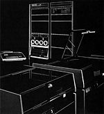
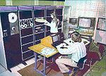
Difference between revisions of "PDP-11/45"
(→KB11-B CPU: add section, board list) |
m (→External links: +pdp11/45 processor handbook) |
||
| (16 intermediate revisions by the same user not shown) | |||
| Line 1: | Line 1: | ||
| − | + | {{Infobox Machine | |
| + | | image = PDP11-45.jpg | ||
| + | | imgwidth = 200px | ||
| + | | caption = A PDP-11/45 | ||
| + | | name = PDP-11/45 | ||
| + | | manufacturer = [[Digital Equipment Corporation|DEC]] | ||
| + | | architecture = [[PDP-11 architecture|PDP-11]] | ||
| + | | form factor = [[minicomputer]] | ||
| + | | word size = 16 bit | ||
| + | | virtual address = 16 bit | ||
| + | | physical address = 18 bit | ||
| + | | design type = [[microcode]]d | ||
| + | | bus arch = [[UNIBUS]]/FastBus | ||
| + | | year introduced = June 1972 | ||
| + | |}} | ||
| + | The '''PDP-11/45''' was the early fast [[UNIBUS]] [[PDP-11]] system, using the [[KB11-A CPU]] (early units, prior to 1976) or [[KB11-D CPU]] (later units) high-performance [[Central Processing Unit|CPUs]], implemented in [[SSI]] [[Schottky TTL]] logic. | ||
| − | + | The difference between the two CPUs was whether they worked with the [[FP11-B Floating-Point Processor|FP11-B]] or [[FP11-C Floating-Point Processor|FP11-C]] [[Floating point processor|FPP]]. The [[FP11 floating point]] was optional, as was the [[KT11-C Memory Management Unit]] (the first implementation of the full [[PDP-11 Memory Management]]). | |
| − | The '''PDP-11/50''' and '''PDP-11/55''' were systems which used the exact same processor, but were configured with MOS or bipolar memory, respectively. | + | The '''PDP-11/50''' and '''PDP-11/55''' were systems which used the exact same processor, but were sold pre-configured with the special high-speed [[MS11 Semiconductor Memory System]] (specific to the PDP-11/45), using 350 nsec [[Metal Oxide Semiconductor|MOS]] or 300 nsec [[bipolar]] memory, respectively. |
| − | + | The machine's 18-bit-address UNIBUS allowed it to have up to 256Kbytes of [[main memory]]. Later non-DEC products such as the [[Able ENABLE]] allowed use of up to 4Mbytes, via an [[Extended UNIBUS]]. | |
| − | + | ==High-speed memory== | |
| − | + | The MS11 high-speed memory was [[multi-port memory|dual-ported]]: one port went to a special high-speed [[bus]] to the CPU (called the Fastbus), which was implemented as part of the CPU's [[backplane]]; the other went to a second UNIBUS (the 'B' UNIBUS). | |
| − | + | That UNIBUS could either be connected to a second PDP-11 (creating a [[multi-processor]] PDP-11 system), or the -11/45's main UNIBUS (the 'A' UNIBUS), so that [[Direct Memory Access|DMA]] devices on that UNIBUS could do [[input/output|I/O]] to the fast memory, which was accessible only from the CPU when the two UNIBUSes were split. | |
| − | + | Note that if the system contained a dual-UNIBUS [[RH11 MASSBUS controller]], devices attached to that could reach the fast memory in a split-UNIBUS system if the RH11's second UNIBUS was attached to the 'B' UNIBUS, giving them a high-speed path to the memory on which there was no contention with the CPU. | |
| − | |||
| − | |||
| − | |||
| − | |||
| − | |||
| − | |||
| − | |||
| − | + | The high-speed memory could be configured in two semi-independent banks, each with its own dual-ported M8110 (later M8120) Semiconductor Memory Control module. | |
| − | + | When the -11/45's CPU went to do a memory cycle, it started cycles on both the FastBus and the 'A' UNIBUS; if that [[address]] was in an MS11, the MS11's controller indicated that it had it, over a special FastBus line. The UNIBUS cycle would then be abandoned before the CPU asserted MSYN. | |
| − | + | A number of products from [[Able Computer]] made use of the FastBus; the [[Able CACHE/45]] (which provided a [[cache]]), and the [[Able SCAT/45]] (which was an MS11 equivalent which could support up to 256 Kbytes of memory). | |
| − | |||
| − | |||
| − | |||
| − | |||
| − | |||
| − | |||
| − | |||
| − | |||
| − | |||
| − | |||
| − | |||
| − | |||
| − | |||
| − | |||
| − | |||
== hampage.hu == | == hampage.hu == | ||
Quoting: | Quoting: | ||
<i> | <i> | ||
| − | Introduced two years after the [[PDP-11/20]], in June 1972. The KB11 was a faster, | + | Introduced two years after the [[PDP-11/20]], in June 1972. The KB11 was a faster, [[microcode]]d CPU built with SSI/MSI (Small/Medium Scale Integration) components. The machine had two different buses: one was a UNIBUS with 18-bit addressing, the other was a fast CPU-memory interconnect. It also introduced split I/D (Instruction/Data) spaces (UNIX used this; the DEC operating systems did not), an MMU (Memory Management Unit) option, an optional FPU (Floating Point Unit). The maximal ammount of memory was 128 Kwords. |
| − | The cycle time of the | + | The cycle time of the PDP-11/45 with bipolar memory (max. 8 KW!) was 300 ns, MOS memories (max. 32 KW) were 450 ns, and core was 980 ns - but without memory management! The MMU added 90 ns to the cycle time. |
| − | The | + | The PDP-11/50 was basically the same machine with different memory. The PDP-11/55 (KB11-D CPU) used the modified CPU of the [[PDP-11/70]], where the cache was left out (instead the memory was the faster bipolar memory). It also had the kernel/supervisor/user operating modes seen on the PDP-11/70, but only had a 18-bit addressing range. It was the fastest of the "classic" PDP-11 CPU's when measured by the cycle times. |
</i> | </i> | ||
| − | == | + | == Gallery == |
| − | |||
| − | |||
| − | |||
[[Image:PDP11-55-geerol.jpg|150px|A PDP-11/55 setup]] | [[Image:PDP11-55-geerol.jpg|150px|A PDP-11/55 setup]] | ||
[[Image:PDP11-55-geerol2.jpg|150px|Different view of the PDP-11/55 setup]] | [[Image:PDP11-55-geerol2.jpg|150px|Different view of the PDP-11/55 setup]] | ||
| Line 64: | Line 54: | ||
[[Image:pdp11-45.jpeg|150px|The "mysterious" PDP-11/45]] | [[Image:pdp11-45.jpeg|150px|The "mysterious" PDP-11/45]] | ||
[[Image:labor114.jpg|150px|11/45 at the Technical University of Budapest: in the foreground you can see a Videoton VDT52100 (VT52-compatible) terminal.]] | [[Image:labor114.jpg|150px|11/45 at the Technical University of Budapest: in the foreground you can see a Videoton VDT52100 (VT52-compatible) terminal.]] | ||
| − | |||
| − | [[ | + | ==External links== |
| + | |||
| + | * [http://www.bitsavers.org/pdf/dec/pdp11/1145/1145_SystemMan.pdf PDP-11/45, 11/50 and 11/55 system user's manual] (EK-1145-OP-001) | ||
| + | * [http://www.bitsavers.org/pdf/dec/pdp11/1145/DEC-11-HMRMA-A-D_PDP-11_45_Maintenance_Reference_Manual_Nov72.pdf PDP-11/45 maintenance reference manual] (DEC-11-HMRMA-A-D) | ||
| + | * [http://www.bitsavers.org/pdf/dec/pdp11/1145/EK-11045-MM-007.pdf PDP-11/45, 11/50 and 11/55 system maintenance manual] (EK-11045-MM-007) | ||
| + | * [http://www.bitsavers.org/pdf/dec/pdp11/1145/PDP-11_45_and_70_Maintenance_Course_Handout_Book_1978.pdf PDP-11/45 /70 Maintenance Course handout book] | ||
| + | * [http://www.bitsavers.org/pdf/dec/pdp11/1145/1145_System_Engineering_Drawings_Jun74.pdf PDP-11/45 system engineering drawings (June 1974)] | ||
| + | * [http://www.bitsavers.org/pdf/dec/pdp11/1145/1145_System_Engineering_Drawings_Jun76.pdf PDP-11/45 system engineering drawings (June 1976)] | ||
| + | * [http://www.bitsavers.org/pdf/dec/pdp11/1155/MP00039_1155vol1_Mar76.pdf 11/55 Vol. 1 Field Maintenance Print Set] (MP00039) | ||
| + | * [http://www.bitsavers.org/pdf/dec/pdp11/handbooks/PDP1145_Handbook_1973.pdf pdp11/45 processor handbook] | ||
| + | |||
| + | {{Nav PDP-11}} | ||
| + | |||
| + | [[Category: UNIBUS PDP-11s]] | ||
Latest revision as of 21:52, 29 February 2024
| PDP-11/45 | |
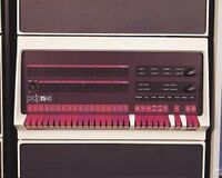 A PDP-11/45 | |
| Manufacturer: | DEC |
|---|---|
| Architecture: | PDP-11 |
| Year Introduced: | June 1972 |
| Form Factor: | minicomputer |
| Word Size: | 16 bit |
| Design Type: | microcoded |
| Physical Address Size: | 18 bit |
| Virtual Address Size: | 16 bit |
| Bus Architecture: | UNIBUS/FastBus |
The PDP-11/45 was the early fast UNIBUS PDP-11 system, using the KB11-A CPU (early units, prior to 1976) or KB11-D CPU (later units) high-performance CPUs, implemented in SSI Schottky TTL logic.
The difference between the two CPUs was whether they worked with the FP11-B or FP11-C FPP. The FP11 floating point was optional, as was the KT11-C Memory Management Unit (the first implementation of the full PDP-11 Memory Management).
The PDP-11/50 and PDP-11/55 were systems which used the exact same processor, but were sold pre-configured with the special high-speed MS11 Semiconductor Memory System (specific to the PDP-11/45), using 350 nsec MOS or 300 nsec bipolar memory, respectively.
The machine's 18-bit-address UNIBUS allowed it to have up to 256Kbytes of main memory. Later non-DEC products such as the Able ENABLE allowed use of up to 4Mbytes, via an Extended UNIBUS.
High-speed memory
The MS11 high-speed memory was dual-ported: one port went to a special high-speed bus to the CPU (called the Fastbus), which was implemented as part of the CPU's backplane; the other went to a second UNIBUS (the 'B' UNIBUS).
That UNIBUS could either be connected to a second PDP-11 (creating a multi-processor PDP-11 system), or the -11/45's main UNIBUS (the 'A' UNIBUS), so that DMA devices on that UNIBUS could do I/O to the fast memory, which was accessible only from the CPU when the two UNIBUSes were split.
Note that if the system contained a dual-UNIBUS RH11 MASSBUS controller, devices attached to that could reach the fast memory in a split-UNIBUS system if the RH11's second UNIBUS was attached to the 'B' UNIBUS, giving them a high-speed path to the memory on which there was no contention with the CPU.
The high-speed memory could be configured in two semi-independent banks, each with its own dual-ported M8110 (later M8120) Semiconductor Memory Control module.
When the -11/45's CPU went to do a memory cycle, it started cycles on both the FastBus and the 'A' UNIBUS; if that address was in an MS11, the MS11's controller indicated that it had it, over a special FastBus line. The UNIBUS cycle would then be abandoned before the CPU asserted MSYN.
A number of products from Able Computer made use of the FastBus; the Able CACHE/45 (which provided a cache), and the Able SCAT/45 (which was an MS11 equivalent which could support up to 256 Kbytes of memory).
hampage.hu
Quoting: Introduced two years after the PDP-11/20, in June 1972. The KB11 was a faster, microcoded CPU built with SSI/MSI (Small/Medium Scale Integration) components. The machine had two different buses: one was a UNIBUS with 18-bit addressing, the other was a fast CPU-memory interconnect. It also introduced split I/D (Instruction/Data) spaces (UNIX used this; the DEC operating systems did not), an MMU (Memory Management Unit) option, an optional FPU (Floating Point Unit). The maximal ammount of memory was 128 Kwords.
The cycle time of the PDP-11/45 with bipolar memory (max. 8 KW!) was 300 ns, MOS memories (max. 32 KW) were 450 ns, and core was 980 ns - but without memory management! The MMU added 90 ns to the cycle time.
The PDP-11/50 was basically the same machine with different memory. The PDP-11/55 (KB11-D CPU) used the modified CPU of the PDP-11/70, where the cache was left out (instead the memory was the faster bipolar memory). It also had the kernel/supervisor/user operating modes seen on the PDP-11/70, but only had a 18-bit addressing range. It was the fastest of the "classic" PDP-11 CPU's when measured by the cycle times.
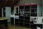
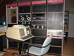
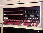
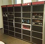
Gallery
External links
- PDP-11/45, 11/50 and 11/55 system user's manual (EK-1145-OP-001)
- PDP-11/45 maintenance reference manual (DEC-11-HMRMA-A-D)
- PDP-11/45, 11/50 and 11/55 system maintenance manual (EK-11045-MM-007)
- PDP-11/45 /70 Maintenance Course handout book
- PDP-11/45 system engineering drawings (June 1974)
- PDP-11/45 system engineering drawings (June 1976)
- 11/55 Vol. 1 Field Maintenance Print Set (MP00039)
- pdp11/45 processor handbook
| v • d • e PDP-11 Computers and Peripherals |
|---|
| UNIBUS PDP-11s - PDP-11/20 • PDP-11/15 • PDP-11/35 • PDP-11/40 • PDP-11/45 • PDP-11/50 • PDP-11/55 • PDP-11/70 PDP-11/05 • PDP-11/10 • PDP-11/04 • PDP-11/34 • PDP-11/60 • PDP-11/44 • PDP-11/24 • PDP-11/84 • PDP-11/94 QBUS PDP-11s - PDP-11/03 • PDP-11/23 • PDP-11/23+ • MicroPDP-11/73 • MicroPDP-11/53 • MicroPDP-11/83 • MicroPDP-11/93 QBUS CPUs: LSI-11 • LSI-11/2 • KDF11-A • KDF11-B • KDJ11-A • KDJ11-B • KDJ11-D • KDJ11-E Buses: UNIBUS • UNIBUS map • SPC • MUD • EUB • QBUS • CD interconnect • PMI Also: PDP-11 architecture • PDP-11 Extended Instruction Set • FP11 floating point • PDP-11 Memory Management |
| UNIBUS CPUs: KA11 • KC11 • KB11-A • KB11-B • KB11-C • KB11-D • KD11-A • KD11-B • KD11-D • KD11-E • KD11-EA • KD11-K • KD11-Z • KDF11-U
Co-processors: FP11-A • FP11-B • FP11-C • FP11-E • FP11-F • KE44-A • FPF11 Chips: LSI-11 • KEV11-A • KEV11-B • KEV11-C • F-11 • KEF11-A • KTF11-A • T-11 • J-11 • FPJ11 CPU options: KE11-E • KE11-F • KJ11-A • KT11-C • KT11-D • KK11-A • KK11-B • KT24 • KTJ11-B Rare CPU options: KS11 Memory Protection and Relocation option • KT11-B Paging Option • KUV11 Writeable Control Store Front panels: KY11-A • KY11-D • KY11-J • KY11-LA • KY11-LB • KY11-P More on buses: UNIBUS and QBUS termination • Bus Arbitration on the Unibus and QBUS • CTI BUS PDT-11s - PDT-11/110 • PDT-11/130 • PDT-11/150 CTI PDP-11s - PRO-325 • PRO-350 • PRO-380 Other: FIS floating point • PDP-11 Commercial Instruction Set • PDP-11 stacks • PDP-11 family differences |
