Difference between revisions of "PDP-11/84"
m (typo) |
m (clarify) |
||
| Line 11: | Line 11: | ||
* UNIBUS adaptor, in slot 4 | * UNIBUS adaptor, in slot 4 | ||
| − | * four [[Small Peripheral Controller|SPC]] slots | + | * four [[Small Peripheral Controller|SPC]] UNIBUS slots |
| − | * three [[Modified UNIBUS Device|MUD]] slots | + | * three [[Modified UNIBUS Device|MUD]] UNIBUS slots |
* UNIBUS 'out' and quad SPC slot, in slot 12 | * UNIBUS 'out' and quad SPC slot, in slot 12 | ||
| − | Note that the PMI slots do not have the [[CD interconnect#Use by PMI|bottom-up]] ordering of PMI-capable slots in a Q22/CD backplane, but are wired as a true bus, allowing the 'CPU, memory, memory' insertion ordering. | + | Note that the PMI slots do not have the [[CD interconnect#Use by PMI|bottom-up]] ordering of PMI-capable slots in a Q22/CD backplane, but are wired as a true bus, allowing the 'CPU, memory, memory' insertion ordering seen here. |
| − | Note also that in the normal configuration (see below for details), the QBUS [[bus grant line]]s are not routed through the memory slots, so if | + | Note also that in the normal configuration (see below for details), the QBUS [[bus grant line]]s are not routed through the memory slots, so if one of these slot is unused, there is no need for a [[jumper]] card in that slot. |
| − | + | As a further feature, on most UNIBUS backplanes, the 'NPG' ([[Direct Memory Access|DMA]] grant line) signal is carried across unused slots by wire jumpers on [[wire-wrap]] pins on the back side of the backplane; on the -11/84 backplane, they are brought out to a [[Dual Inline Package|DIP]] switch on the MDM module, for easier configuration changes. | |
==QBUS slots== | ==QBUS slots== | ||
| Line 29: | Line 29: | ||
There are indeed two jumpers, W1 and W2 (in the upper right-hand corner, when facing the backplane from the board insertion side); the traces connected to them are on the surface, so it is possible to see where they go: one end runs to a trace connected from slot 1 to slot 2, and the other to a trace connected from slot 3 to slot 4; those connect to AM2 (BIAKI) and AN2 (BIAKO), and AR2 (BDMGI) and AS2 (BDMGO). | There are indeed two jumpers, W1 and W2 (in the upper right-hand corner, when facing the backplane from the board insertion side); the traces connected to them are on the surface, so it is possible to see where they go: one end runs to a trace connected from slot 1 to slot 2, and the other to a trace connected from slot 3 to slot 4; those connect to AM2 (BIAKI) and AN2 (BIAKO), and AR2 (BDMGI) and AS2 (BDMGO). | ||
| − | Thus, when the jumpers are in, the CPU's BIAKO/BDMGO pins are connected directly to the UNIBUS adapter's BIAKI/BDMGI pins; when they are out, those signals are routed through the two 'memory' slots, in the normal QBUS manner | + | Thus, when the jumpers are in, the CPU's BIAKO/BDMGO pins are connected directly to the UNIBUS adapter's BIAKI/BDMGI pins; when they are out, those signals are routed through the two 'memory' slots, in the normal QBUS manner. |
| − | As to why DEC put this capability in, and then didn't more widely document it, or use it: that is not known. Perhaps they thought it would introduce extra complixity in the user instructions, or something | + | It therefore seems those two slots ''can'' function as real QBUS slots. (If not, why arrange things so that the can run grant lines through them?) As far as is known, this has not yet been verified, though. |
| + | |||
| + | As to why DEC put this capability in, and then didn't more widely document it, or use it: that is not known. Perhaps they thought it would introduce extra complixity in the user instructions, or something? | ||
== hampage.hu == | == hampage.hu == | ||
Revision as of 16:50, 5 July 2018
The PDP-11/84 is the UNIBUS-capable twin to the QBUS-only PDP-11/83; both used the KDJ11-B CPU (with its PMI bus). The -11/84 added a KTJ11-B UNIBUS adapter to provide its UNIBUS, and had a main backplane which was half QBUS, and half UNIBUS, with a slot in the middle for the KTJ11-B.
The backplane contains (in order) four quad-height slots, the first of which is a custom slot, and the others are PMI (technically Q22/CD, although slightly modified from the normal form of that in this backplane, see below); they are used for (in order, from the front of the machine):
- the Machine Debug Monitor board (M7677); this slot is not numbered
- the CPU board; this is slot 1
- main memory board
- optional second main memory board
and nine hex-height slots, used for:
- UNIBUS adaptor, in slot 4
- four SPC UNIBUS slots
- three MUD UNIBUS slots
- UNIBUS 'out' and quad SPC slot, in slot 12
Note that the PMI slots do not have the bottom-up ordering of PMI-capable slots in a Q22/CD backplane, but are wired as a true bus, allowing the 'CPU, memory, memory' insertion ordering seen here.
Note also that in the normal configuration (see below for details), the QBUS bus grant lines are not routed through the memory slots, so if one of these slot is unused, there is no need for a jumper card in that slot.
As a further feature, on most UNIBUS backplanes, the 'NPG' (DMA grant line) signal is carried across unused slots by wire jumpers on wire-wrap pins on the back side of the backplane; on the -11/84 backplane, they are brought out to a DIP switch on the MDM module, for easier configuration changes.
QBUS slots
The two main memory slots can in fact be configured as regular Q22/CD QBUS slots, by removing two jumpers. EK-PDP84-TM-PR4 (PDP-11/84 Technical Manual) says (in section 2.1.14, "Backplane (H9277-A)", pg. 2-6):
- Bus signals BDMGI (pin AR2) and BIAKI (pin AM2) for slots 2 & 3 are jumpered on the front of the backplane.
There are indeed two jumpers, W1 and W2 (in the upper right-hand corner, when facing the backplane from the board insertion side); the traces connected to them are on the surface, so it is possible to see where they go: one end runs to a trace connected from slot 1 to slot 2, and the other to a trace connected from slot 3 to slot 4; those connect to AM2 (BIAKI) and AN2 (BIAKO), and AR2 (BDMGI) and AS2 (BDMGO).
Thus, when the jumpers are in, the CPU's BIAKO/BDMGO pins are connected directly to the UNIBUS adapter's BIAKI/BDMGI pins; when they are out, those signals are routed through the two 'memory' slots, in the normal QBUS manner.
It therefore seems those two slots can function as real QBUS slots. (If not, why arrange things so that the can run grant lines through them?) As far as is known, this has not yet been verified, though.
As to why DEC put this capability in, and then didn't more widely document it, or use it: that is not known. Perhaps they thought it would introduce extra complixity in the user instructions, or something?
hampage.hu
Quoting: Introduced in 1988. Based on the J-11 chip set, DEC originally wanted the clock speed to be 20MHz, but it couldn't be done on time, so the actual speed was 18MHz. It was the fastest CPU of the PDP-11's anyhow. The high-end configuration had up to 4MB RAM on PMI (Private Memory Interconnect) and a floating-point accelerator.
The UNIBUS-based PDP-11/84 was for those customers, who wanted more I/O throughput or had some legacy equipment.
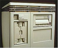
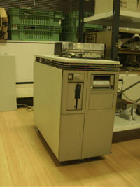
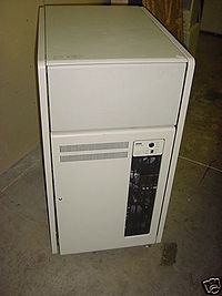
The box on the picture to the left is a BA123 which was a popular enclosure for qbus machines. Apart from the 12x4-slot qbus backplane, it had five slots for storage units, e.g. room for two or three harddisks, a tape drive (TK50 here) and floppy.
Gallery
| v • d • e PDP-11 Computers and Peripherals |
|---|
| UNIBUS PDP-11s - PDP-11/20 • PDP-11/15 • PDP-11/35 • PDP-11/40 • PDP-11/45 • PDP-11/50 • PDP-11/55 • PDP-11/70 PDP-11/05 • PDP-11/10 • PDP-11/04 • PDP-11/34 • PDP-11/60 • PDP-11/44 • PDP-11/24 • PDP-11/84 • PDP-11/94 QBUS PDP-11s - PDP-11/03 • PDP-11/23 • PDP-11/23+ • MicroPDP-11/73 • MicroPDP-11/53 • MicroPDP-11/83 • MicroPDP-11/93 QBUS CPUs: LSI-11 • LSI-11/2 • KDF11-A • KDF11-B • KDJ11-A • KDJ11-B • KDJ11-D • KDJ11-E Buses: UNIBUS • UNIBUS map • SPC • MUD • EUB • QBUS • CD interconnect • PMI Also: PDP-11 architecture • PDP-11 Extended Instruction Set • FP11 floating point • PDP-11 Memory Management |
| UNIBUS CPUs: KA11 • KC11 • KB11-A • KB11-B • KB11-C • KB11-D • KD11-A • KD11-B • KD11-D • KD11-E • KD11-EA • KD11-K • KD11-Z • KDF11-U
Co-processors: FP11-A • FP11-B • FP11-C • FP11-E • FP11-F • KE44-A • FPF11 Chips: LSI-11 • KEV11-A • KEV11-B • KEV11-C • F-11 • KEF11-A • KTF11-A • T-11 • J-11 • FPJ11 CPU options: KE11-E • KE11-F • KJ11-A • KT11-C • KT11-D • KK11-A • KK11-B • KT24 • KTJ11-B Rare CPU options: KS11 Memory Protection and Relocation option • KT11-B Paging Option • KUV11 Writeable Control Store Front panels: KY11-A • KY11-D • KY11-J • KY11-LA • KY11-LB • KY11-P More on buses: UNIBUS and QBUS termination • Bus Arbitration on the Unibus and QBUS • CTI BUS PDT-11s - PDT-11/110 • PDT-11/130 • PDT-11/150 CTI PDP-11s - PRO-325 • PRO-350 • PRO-380 Other: FIS floating point • PDP-11 Commercial Instruction Set • PDP-11 stacks • PDP-11 family differences |


