Difference between revisions of "PDP-11/70"
(Add main memory systems) |
(Link a few terms) |
||
| Line 14: | Line 14: | ||
The '''PDP-11/70''' was a very high performance [[UNIBUS]] [[PDP-11]] system; it basically took the high-performance CPU of the [[PDP-11/45]] (implemented in [[SSI]] [[Schottky TTL]] logic), and augmented it with: | The '''PDP-11/70''' was a very high performance [[UNIBUS]] [[PDP-11]] system; it basically took the high-performance CPU of the [[PDP-11/45]] (implemented in [[SSI]] [[Schottky TTL]] logic), and augmented it with: | ||
| − | * A 2 Kbyte, 300 nsec cache, organized as 2-way set associative, with 4-byte blocks, connected to what had been the FastBus high-speed memory interface on the PDP-11/45 CPU | + | * A 2 Kbyte, 300 nsec [[cache]], organized as 2-way set associative, with 4-byte blocks, connected to what had been the FastBus high-speed memory interface on the PDP-11/45 CPU |
* The ability to support up to 4 Mbytes of memory via a new Main Memory Bus, and changes to the CPU to allow access to that much memory | * The ability to support up to 4 Mbytes of memory via a new Main Memory Bus, and changes to the CPU to allow access to that much memory | ||
| − | * A UNIBUS map to allow devices on the UNIBUS access to all of that memory | + | * A [[UNIBUS map]] to allow devices on the UNIBUS access to all of that memory |
* The ability to support up to 4 [[MASSBUS]] adapters, which connected high-speed mass storage devices directly to the [[main memory]], bypassing the UNIBUS | * The ability to support up to 4 [[MASSBUS]] adapters, which connected high-speed mass storage devices directly to the [[main memory]], bypassing the UNIBUS | ||
| − | The CPU was the KB11-B (early units, prior to 1976) or KB11-C (later) CPU. (The difference between the two was whether they worked with the optional [[FP11-B]] or [[FP11-C]] [[Floating point processor|FPP]].) | + | The CPU was the KB11-B (in early units, prior to 1976) or KB11-C (later) CPU. (The difference between the two was whether they worked with the optional [[FP11-B]] or [[FP11-C]] [[Floating point processor|FPP]].) |
The main memory systeme supported by the -11/70 were the [[MJ11 memory system]] (which used [[core memory]]), and the later [[MK11 memory system]] (which used [[DRAM]]). | The main memory systeme supported by the -11/70 were the [[MJ11 memory system]] (which used [[core memory]]), and the later [[MK11 memory system]] (which used [[DRAM]]). | ||
| Line 74: | Line 74: | ||
{{PDP-11}} | {{PDP-11}} | ||
| − | + | ||
| + | [[Category:UNIBUS PDP-11s]] | ||
Revision as of 13:15, 17 February 2018
| PDP-11/70 | |
| Manufacturer: | Digital Equipment Corporation |
|---|---|
| Year Introduced: | March 1975 |
| Word Size: | 16 bit |
| Physical Address Size: | 22 bit |
| Virtual Address Size: | 16 bit |
| Bus Architecture: | UNIBUS/MASSBUS/memory bus |
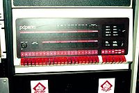
The PDP-11/70 was a very high performance UNIBUS PDP-11 system; it basically took the high-performance CPU of the PDP-11/45 (implemented in SSI Schottky TTL logic), and augmented it with:
- A 2 Kbyte, 300 nsec cache, organized as 2-way set associative, with 4-byte blocks, connected to what had been the FastBus high-speed memory interface on the PDP-11/45 CPU
- The ability to support up to 4 Mbytes of memory via a new Main Memory Bus, and changes to the CPU to allow access to that much memory
- A UNIBUS map to allow devices on the UNIBUS access to all of that memory
- The ability to support up to 4 MASSBUS adapters, which connected high-speed mass storage devices directly to the main memory, bypassing the UNIBUS
The CPU was the KB11-B (in early units, prior to 1976) or KB11-C (later) CPU. (The difference between the two was whether they worked with the optional FP11-B or FP11-C FPP.)
The main memory systeme supported by the -11/70 were the MJ11 memory system (which used core memory), and the later MK11 memory system (which used DRAM).
Contents
KB11-B CPU
The KB11-B board set included:
- M8130 Data Paths
- M8131 General Registers and ALU control
- M8132 Instruction Register Decode and Condition Codes
- M8133 ROM and ROM Control
- M8134 Processor Data and UNIBUS Registers
- M8135 Trap and Miscellaneous Control
- M8136 UNIBUS and Console Control
- M8137 System Address Paths
- M8138 System Status Registers
- M8139 Timing Generator
- M8140 System Descriptor and Console Cables
- M8141 UNIBUS Map
- M8142 Cache Control
- M8143 Cache Address Memory
- M8144 Cache Data Memory
- M8145 Cache Data paths
KB11-C CPU
The KB11-C board set included many of the same boards as the KB11-B, with the following differences:
- The M8133 ROM and ROM Control was replaced with the M8123
- The M8138 System Status Registers was replaced with the M8138-YA
Note: The DEC documentation contains an error here. The 11/70 Maintenance Manual (EK-11070-MM-002) says (pg. 1-3) that the KB11-C contains an M8133 ROM and ROM Control board, but the KB11-C Engineering Drawings include the drawings for the M8123, not the M8133; other manuals also confirm that the KB11-C uses the M8123 (see, for example, the KB11-A,D Maintainence Manual, EK-KB11A-MM-004, pg 1-1).
hampage.hu
Quote: Introduced in March 1975, the PDP-11/70 is the bigest of the PDP-11s. The KB11B is a re-enginered version of the PDP-11/45's CPU, with some new features. Two of the most important changes was the addition of cache (2 KByte of bipolar memory) and the 22-bit memory management. The latter enables the usage of memory up to 2 Mwords, using the UNIBUS map, which translates 18-bit UNIBUS addresses to 22-bit physical addresses. The kernel/supervisor/user operating modes and the MMU was standard. Important options: FPP, MASSBUS adapters (RH70's, up to four) with direct memory access.
The original processor had the floating point unit of the PDP-11/45, which turned out to be ineffective, so it was resdesigned (KB11C). Overall performance is 0.6th of the VAX-11/780.
A normal system occupied at least two H960 cabinets (memory and CPU), the UNIBUS expansion needed another. There were also later revisions sold in another cabinet, without the front panel (Datasystem 570?).
Trivia: The original business plan called for 1000 PDP-11/70's to be built, it was supposed to be a "stopgap" until the "wide word machine" came out. This "word wide machine" was originally a small PDP-10 (36-bit machine), but it was then cancelled in favor of the 32-bit VAX. Anyhow, more than 10,000 PDP-11/70's were built.
Gallery
| v • d • e PDP-11 Computers and Peripherals |
|---|
| UNIBUS PDP-11s - PDP-11/20 • PDP-11/15 • PDP-11/35 • PDP-11/40 • PDP-11/45 • PDP-11/50 • PDP-11/55 • PDP-11/70 PDP-11/05 • PDP-11/10 • PDP-11/04 • PDP-11/34 • PDP-11/60 • PDP-11/44 • PDP-11/24 • PDP-11/84 • PDP-11/94 QBUS PDP-11s - PDP-11/03 • PDP-11/23 • PDP-11/23+ • MicroPDP-11/73 • MicroPDP-11/53 • MicroPDP-11/83 • MicroPDP-11/93 QBUS CPUs: LSI-11 • LSI-11/2 • KDF11-A • KDF11-B • KDJ11-A • KDJ11-B • KDJ11-D • KDJ11-E Buses: UNIBUS • UNIBUS map • SPC • MUD • EUB • QBUS • CD interconnect • PMI Also: PDP-11 architecture • PDP-11 Extended Instruction Set • FP11 floating point • PDP-11 Memory Management |
| UNIBUS CPUs: KA11 • KC11 • KB11-A • KB11-B • KB11-C • KB11-D • KD11-A • KD11-B • KD11-D • KD11-E • KD11-EA • KD11-K • KD11-Z • KDF11-U
Co-processors: FP11-A • FP11-B • FP11-C • FP11-E • FP11-F • KE44-A • FPF11 Chips: LSI-11 • KEV11-A • KEV11-B • KEV11-C • F-11 • KEF11-A • KTF11-A • T-11 • J-11 • FPJ11 CPU options: KE11-E • KE11-F • KJ11-A • KT11-C • KT11-D • KK11-A • KK11-B • KT24 • KTJ11-B Rare CPU options: KS11 Memory Protection and Relocation option • KT11-B Paging Option • KUV11 Writeable Control Store Front panels: KY11-A • KY11-D • KY11-J • KY11-LA • KY11-LB • KY11-P More on buses: UNIBUS and QBUS termination • Bus Arbitration on the Unibus and QBUS • CTI BUS PDT-11s - PDT-11/110 • PDT-11/130 • PDT-11/150 CTI PDP-11s - PRO-325 • PRO-350 • PRO-380 Other: FIS floating point • PDP-11 Commercial Instruction Set • PDP-11 stacks • PDP-11 family differences |


