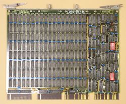
MSV11-Q QBUS memory
The MSV11-Q (M7551) is a quad-height QBUS DRAM main memory card. Initially it used 64Kx1 DRAM chips, later ones uses 256Kx1 DRAMs. The memory is arranged as 8 banks, each 16 data bits (1 PDP-11 word) wide, with 2 additional bits for parity (1 per byte).
It holds 1 MByte with 64K DRAMs; 4 Mbytes when fully populated with 256K DRAMs, or 2 Mbytes when half-populated (the only partially-filled configuration allowed). Three versions exist:
- MSV11-QA, 1 Mbyte (64K DRAMs)
- MSV11-QB, 2 Mbytes (256K DRAMs)
- MSV11-QC, 4 Mbytes (256K DRAMs)
all are Q22, and support block mode. The -QA comes in two etch revisions; the latter version supports battery backup. The -QB and -QC are the same etch as the later -QA.
Control Register
Each board has a single control register, which can be configured in the range 172100-172136.
In the register contents (below), all the bits can be read and written by software; most are cleared by power up and bus INIT. Bits which can only be modified by the CPU are shown in normal font, and those which can also be set by the hardware in italics.
| Parity Error | Extended Error Address Enable | Reserved | Error Address | Reserved | Write Wrong Parity | Reserved | Parity Error Enable | ||||||||
| 15 | 14 | 13 | 12 | 11 | 10 | 09 | 08 | 07 | 06 | 05 | 04 | 03 | 02 | 01 | 00 |
The 'Error Address' field contents depend on the setting of the 'Extended Error Address Enable' bit; when it holds the low address ('Extended Error Address Enable' is 0), it holds address bits 11 through 17; when it holds the high address ('Extended Error Address Enable' is 1), it holds bits 21 through 18 - bits 11-9 of the register are unused.
Technical information
As far as is known, there are no copies of the engineering drawings extant for the MSV11-Q. However, some technical information, enough to repair boards with faulty DRAM chips, has been gathered on it, and that is made available here.
As described above, each board has 8 (sometimes 4) banks in the array of DRAM chips; with 64K chips, each bank is thus 128KB; with 256K chips, they are 512KB.
The chips in each bank run across the board (when it is oriented with the chip side facing the viewer, with the metal edging holding the handles at the bottom). Bit 0 (value 1) is on the right hand edge of the array; bit 15 (value 0100000) is on the left, with the two parity bits in the middle.
The following 64K DRAM chips have been observed to be used: M5K4164ANP-15P (Micron Technologies), NEC D4164C211 (NEC Electronics).
Further reading
- MSV11-QA, MSV11-QB, and MSV11-QC Field Maintenance Printset (MP-01931)
| v • d • e PDP-11 Computers and Peripherals |
|---|
| UNIBUS PDP-11s - PDP-11/20 • PDP-11/15 • PDP-11/35 • PDP-11/40 • PDP-11/45 • PDP-11/50 • PDP-11/55 • PDP-11/70 PDP-11/05 • PDP-11/10 • PDP-11/04 • PDP-11/34 • PDP-11/60 • PDP-11/44 • PDP-11/24 • PDP-11/84 • PDP-11/94 QBUS PDP-11s - PDP-11/03 • PDP-11/23 • PDP-11/23+ • MicroPDP-11/73 • MicroPDP-11/53 • MicroPDP-11/83 • MicroPDP-11/93 QBUS CPUs: LSI-11 • LSI-11/2 • KDF11-A • KDF11-B • KDJ11-A • KDJ11-B • KDJ11-D • KDJ11-E Buses: UNIBUS • UNIBUS map • SPC • MUD • EUB • QBUS • CD interconnect • PMI Also: PDP-11 architecture • PDP-11 Extended Instruction Set • FP11 floating point • PDP-11 Memory Management |
| UNIBUS CPUs: KA11 • KC11 • KB11-A • KB11-B • KB11-C • KB11-D • KD11-A • KD11-B • KD11-D • KD11-E • KD11-EA • KD11-K • KD11-Z • KDF11-U
Co-processors: FP11-A • FP11-B • FP11-C • FP11-E • FP11-F • KE44-A • FPF11 Chips: LSI-11 • KEV11-A • KEV11-B • KEV11-C • F-11 • KEF11-A • KTF11-A • T-11 • J-11 • FPJ11 CPU options: KE11-E • KE11-F • KJ11-A • KT11-C • KT11-D • KK11-A • KK11-B • KT24 • KTJ11-B Rare CPU options: KS11 Memory Protection and Relocation option • KT11-B Paging Option • KUV11 Writeable Control Store Front panels: KY11-A • KY11-D • KY11-J • KY11-LA • KY11-LB • KY11-P More on buses: UNIBUS and QBUS termination • Bus Arbitration on the Unibus and QBUS • CTI BUS PDT-11s - PDT-11/110 • PDT-11/130 • PDT-11/150 CTI PDP-11s - PRO-325 • PRO-350 • PRO-380 Other: FIS floating point • PDP-11 Commercial Instruction Set • PDP-11 stacks • PDP-11 family differences |
