Difference between revisions of "MK11 memory system"
m (→CSR Access: clarify) |
(→CSR Access: One guess at the -11/70 modification) |
||
| Line 35: | Line 35: | ||
The control [[register]]s for the MK11 have [[address]]es in the I/O page of the PDP-11 [[UNIBUS]] [[address space]]; but the MK11 is not on the UNIBUS, so a 'trick' is needed for the [[Central Processing Unit|CPU]] to be able to gain access to them. That is to use the [[UNIBUS map]] (usually used for [[Direct Memory Access|DMA]] cycles from [[peripheral|device]]s to main memory); the [[memory management]] and UNIBUS map are set up so that CPU references to the CSRs are routed out to the UNIBUS, and then back in to the MK11. | The control [[register]]s for the MK11 have [[address]]es in the I/O page of the PDP-11 [[UNIBUS]] [[address space]]; but the MK11 is not on the UNIBUS, so a 'trick' is needed for the [[Central Processing Unit|CPU]] to be able to gain access to them. That is to use the [[UNIBUS map]] (usually used for [[Direct Memory Access|DMA]] cycles from [[peripheral|device]]s to main memory); the [[memory management]] and UNIBUS map are set up so that CPU references to the CSRs are routed out to the UNIBUS, and then back in to the MK11. | ||
| − | The process for doing so from the [[front panel]] is given in the 'MK11 MOS memory technical manual', section 6.3.4, 'CSR Addressing'. That section also cryptically alludes to a "direct addressing" method (the use of the UNIBUS map, above, is referred to as an "indirect addressing" method), but it requires a "modified PDP-11/70 processor", of which no details are given. | + | The process for doing so from the [[front panel]] is given in the 'MK11 MOS memory technical manual', section 6.3.4, 'CSR Addressing'. That section also cryptically alludes to a "direct addressing" method (the use of the UNIBUS map, above, is referred to as an "indirect addressing" method), but it requires a "modified PDP-11/70 processor", of which no details are given (one ''hypothesis'' is that a portion of the I/O page in the CPU's address space is sent out the memory bus, not through KPAR7). |
==Upgrades== | ==Upgrades== | ||
Revision as of 22:35, 4 March 2021
The MK11 memory system was a DRAM main memory system for the PDP-11/70. It was 32 bits wide, to interface to the -11/70's Main Memory Bus, and provided ECC (7 bits/double-word), which could correct all single-bit errors. Read, Write, and Exchange cycles were supported. It came in at least three variants:
- the MK11-B (which used 32KB and 64KB MS11-K MOS memory array modules)
- the MK11-B-2 (which added the ability to use 256KB memory array modules).
- the MKA11 (a multi-port memory version for the PDP-11/74)
(It is not known if there was an MK11-A, and if so, what it was.)
A maximum of eight MK11 systems could be installed on a single machine, for a maximum of slightly less than 4MB (with 64KB modules, eight MK11 systems would be needed to reach this; with 265KB modules, only two).
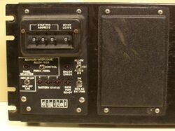
An MK11 system contained six hex control modules (of four different types), and then a group of up to eight pairs of hex memory array modules; they were housed in a BA11-K mounting box, and plugged into a large custom backplane. A separate 'Box Controller' panel module mounted in the rack controlled whether the MK11 unit was in use, what its starting address was, 'external' interleaving, etc.
(The MK11 contains two controllers internally, and when an MK11 contains a symmetrical set of memory array modules, 'internal' interleaving between the two of them is automagically enabled.)
Contents
Implementation
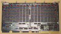
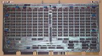
A backplane held a pair of memory bus interface boards (an M8158 address buffer board, and either an M8159 or M8164 data buffer board; the M8159 could only be used with 64KB memory modules, whereas the M8164 could be used with either those or 256KB modules); two pairs of control boards (an M8160 Control A module, and an M8161 Control B module), one set for each controller of the MK11 system; and between 1 and 16 memory array modules.
The Control A modules generated timing signals, did module addressing, checked the configuration (below), and did memory refresh. The Control B modules interfaced to the memory modules, and computed and checked the ECC.
The memory array modules were placed in the backplane from the inner slots (next to the buffer and control boards) toward the outer; the buffer and control boards went in the center slots.
When an MK11 backplane contained a mix of different size board pairs, the smallest ones had to be in the lower locations (i.e. close to the buffer and control boards). If there were an even number of memory array boards installed, and the sizes were matched on each side, the MK11 automatically enabled interleaving.
The MKA11 added two other control boards: the M8162 Port MUX A module, and the M8163 Port MUX B module.
Cabling
The Box Controller panel (DEC part number 70-14274-0) was connected to the MK11 via two cables: a BC08R-10 flat cable (which plugs into Berg connector header J5 on the M8159 data buffer board), and a power control cable (DEC part number 70-14311-9F).
CSR Access
The control registers for the MK11 have addresses in the I/O page of the PDP-11 UNIBUS address space; but the MK11 is not on the UNIBUS, so a 'trick' is needed for the CPU to be able to gain access to them. That is to use the UNIBUS map (usually used for DMA cycles from devices to main memory); the memory management and UNIBUS map are set up so that CPU references to the CSRs are routed out to the UNIBUS, and then back in to the MK11.
The process for doing so from the front panel is given in the 'MK11 MOS memory technical manual', section 6.3.4, 'CSR Addressing'. That section also cryptically alludes to a "direct addressing" method (the use of the UNIBUS map, above, is referred to as an "indirect addressing" method), but it requires a "modified PDP-11/70 processor", of which no details are given (one hypothesis is that a portion of the I/O page in the CPU's address space is sent out the memory bus, not through KPAR7).
Upgrades
An MK11-B could be upgraded to an MK11-B-2 by swapping in an M8164 data buffer board for the M8159, and swapping in, or adding, pairs of 256KB board sets.
There were two generations of memory array modules for the MK11; the first is the MS11-K (link above; 32KB and 64KB, depending on the number of DRAM chips used); the second is the M8728 (name currently unknown), which used 156 16Kx1 DRAM chips to provide a 256KB memory array module.
Non-standard upgrades
A later board, the M8750, used the same PCB as the M8728, but 64Kx1 DRAM chips - the board had jumpers to allow the use of either size chip - to provide a 1MB memory array module (used in the VAX-11/730 and VAX-11/750).
This board was not supported by the MK11. However, it is possible to use them in an MK11, with slight modifications (see the message linked below for the details).
Also, it is theorized that with the appropriate jumper configuration, they can be made to look like 256KB boards; this will 'waste' 3/4 of the storage on the card, but if 256KB boards are unobtainable, the fairly widely-available M8750's could be substituted.
Further reading
- MK11 MOS memory technical manual, EK-0MK11-TM-001
See also
External links
| v • d • e PDP-11 Computers and Peripherals |
|---|
| UNIBUS PDP-11s - PDP-11/20 • PDP-11/15 • PDP-11/35 • PDP-11/40 • PDP-11/45 • PDP-11/50 • PDP-11/55 • PDP-11/70 PDP-11/05 • PDP-11/10 • PDP-11/04 • PDP-11/34 • PDP-11/60 • PDP-11/44 • PDP-11/24 • PDP-11/84 • PDP-11/94 QBUS PDP-11s - PDP-11/03 • PDP-11/23 • PDP-11/23+ • MicroPDP-11/73 • MicroPDP-11/53 • MicroPDP-11/83 • MicroPDP-11/93 QBUS CPUs: LSI-11 • LSI-11/2 • KDF11-A • KDF11-B • KDJ11-A • KDJ11-B • KDJ11-D • KDJ11-E Buses: UNIBUS • UNIBUS map • SPC • MUD • EUB • QBUS • CD interconnect • PMI Also: PDP-11 architecture • PDP-11 Extended Instruction Set • FP11 floating point • PDP-11 Memory Management |
| UNIBUS CPUs: KA11 • KC11 • KB11-A • KB11-B • KB11-C • KB11-D • KD11-A • KD11-B • KD11-D • KD11-E • KD11-EA • KD11-K • KD11-Z • KDF11-U
Co-processors: FP11-A • FP11-B • FP11-C • FP11-E • FP11-F • KE44-A • FPF11 Chips: LSI-11 • KEV11-A • KEV11-B • KEV11-C • F-11 • KEF11-A • KTF11-A • T-11 • J-11 • FPJ11 CPU options: KE11-E • KE11-F • KJ11-A • KT11-C • KT11-D • KK11-A • KK11-B • KT24 • KTJ11-B Rare CPU options: KS11 Memory Protection and Relocation option • KT11-B Paging Option • KUV11 Writeable Control Store Front panels: KY11-A • KY11-D • KY11-J • KY11-LA • KY11-LB • KY11-P More on buses: UNIBUS and QBUS termination • Bus Arbitration on the Unibus and QBUS • CTI BUS PDT-11s - PDT-11/110 • PDT-11/130 • PDT-11/150 CTI PDP-11s - PRO-325 • PRO-350 • PRO-380 Other: FIS floating point • PDP-11 Commercial Instruction Set • PDP-11 stacks • PDP-11 family differences |


